Thursday, June 30, 2022

First session removing grease and oil from the 1053

FOUND TIME BETWEEN THE SPRINKLES TO SET UP OUTSIDE MY SHOP

We had some light rain in the morning and slightly heavier thunderstorms in the afternoon, but I did have a window when I could set up the container, the typewriter mechanism and load up the lacquer thinner into the syringe. 

REMOVING GREASE ALONG THE OPERATIONAL SHAFT AND FUNCTION CLUTCHES

One long shaft runs from left to right in the Selectric typewriter, coupled by a rubber belt to the continuously running motor behind it. The right side rotates at all time, but just to the left of midline there is a clutch which keeps the left side from rotating until the clutch is tripped.

The left side rotates to cause a print cycle. The whiffletree selection mechanism chooses an amount of tilt and of rotate, the ball accomplishes those movements, then the ball is hurled forward towards the ribbon just in front of the paper on the platen. At the end of a rotation the clutch latches up to wait for a later request for the next character to be typed. 

The right side runs all the time but has a several clutches on it that will transfer the rotary movement of the operational shaft to levers and other mechanisms mounted towards the rear of the typewriter. These clutches are tripped by a lever coming from pushbuttons and the solenoids mounted in front of the operational shaft on the right side. The clutch spins either half a rotation or a full rotation, depending on the design of that clutch, then latches up to wait for the next triggering event. 

Each clutch and all the levers that trip it, latch it at the end, and transfer motion to the function activation mechanisms require old lubricants to be removed in order to operate freely again. I squirted the solvent along the operational shaft, on the clutch mechanisms and the related levers. It dripped down into the plastic container under the typewriter. 

I had to ensure that the solvent spray and drip wouldn't reach the solenoids in front of the operational shaft, nor the solenoids on the left side that select the whiffletree to set rotate and tilt for printing. Finally I had to avoid the motor itself in the rear. This means that I had to hold the mechanism carefully at the proper angles and be judicious in the application of the solvent. 

After flushing, the parts have to be moved a bit to get into the tightest pockets where grease or oil remains. A second spray as they are moved ensures they are cleaned well. Finally I put on a small amount of the Nye clock oil to ensure these joints all moved freely. 

STATUS AFTER FIRST ROUND OF CLEANING

I was able to get the operational shaft to rotate quite freely. Backspace trigger mechanism is tripping one of the clutches. I can coax it to its latched position (the trigger) which stops the clutch cycles but if it is activated it doesn't unlatch properly. Most likely sludge somewhere in the linkage but could also be a missing spring which forces the trigger forward to latch again. 

The print cycle clutch was frozen solid. All the levers and other parts of the mechanism were almost impossible to move until I worked them with Nye Oil after some degreasing. It still won't trip a cycle, so there may be sludge inside the clutch itself causing problems. So far I haven't been able to trip a print cycle which should be easy to do manually. 

Results of reloading the hi core diagnostic section for routine 2 - address testing

RELOADED THE SECTION OF CORE THAT CONTAINS ROUTINE 2 CODE, DATA AND SUBS

Because it was more likely that we had an error in loading the test code or data, rather than a hardware error in addressing, I trimmed the load file and ran the Memory Load Tool again. Since the critical sections aren't that big, I then stepped through core displaying the contents to verify it was correct.

RUN ROUTINE 2 TO CHECK THE ADDRESSING LOGIC OF MEMORY

This routine loops from address 0800 up to the top of memory and wraps around to the first ten locations of low core. It writes its address into each word. After the write loop, it loops again reading each location and verifying that the contents match the address. A second version is run storing the complement of the address in each word and checking it again. 

RESULTS OF THE TEST AND CONCLUSIONS

It ran flawlessly through all six routines! The memory that was tested is all good. For completeness, I have to run the Lo Core diagnostic. That is essentially the same code but it sits up in /0800 and above, thus it can test all the low memory and wrap around to some of the high addresses.

FIRST TRY OF LO CORE HAD SIMILAR ERRORS AS THE INITIAL HI CORE TESTS

My memory loader tool toggled in the Lo Core diagnostic after which I set the IAR to 0961, its start address and hit run. It did properly detect that this was an 8K machine, but when I hit run to start the tests it kept stopping on a word of 0000 that was clearly intended to hold a valid instruction. I got past that and again saw the 3004 and 3005 error waits for routine 2, similar to but not exactly the same as with the corrupted Hi Core test. 


RELOADED ROUTINE 2 CODE, DATA AND SUBROUTINES AGAIN

I stripped down the load file and used the Memory Load Tool to replace those sections of core with the contents. Since this had fixed the Hi Core problem, I didn't hand verify the data this time, I just ran it again.

RERUN OF LO CORE DIAGNOSTIC WAS FULLY SUCCESSFUL

This time, after starting at 0961 and seeing the proper core size in the register, I started looping on routine 2, without any error waits, then let it run all six runs to completion. The machine passed, just as it had with the Hi Core program which means that we exercised all of core memory with no errors detected. I now declare the memory and CPU fully functional. 


NEXT STEPS

My next steps are restoration of two peripherals and debugging of their controller circuits. The 1053 Console Printer is the immediate priority, then I can dive into the internal disk drive to complete the restoration of this machine. 

Beginning the de-gunking of the IBM 1130 console typewriter

REMOVING SOLIDIFIED OR THICK LUBRICANTS FROM THE 1053

Both oils and greases that IBM used with their equipment in the 1960s and 1970s age poorly. I suspect that lighter factions of petroleum are slowly evaporating, leaving only the thickest portions. Also, atmospheric dust gets trapped in the grease or oil over time which creates a kind of paste that increases the friction. 

Regardless of the precise set of processes that produce the effect, it eventually adds so much resistance that moving parts don't turn as they should. Springs pull levers back into position but when the oil stiffens so much, it either moves at a snails pace or won't fully return. Shafts with many parts that move on them, such as the main operational shaft of the typewriter, fail to turn at all due to the cumulative drag. 

In the old days, IBM technicians would submerge the entire mechanism in a bath of triclorethylene which dissolved all the greases and oils. The machine would be relubricated with new oils and grease after this cleaning. Alas, we now know that TCE is carcinogenic and it is no longer on hand for cleaning.

Most selectric mechanisms can be dunked in other cleaners such as acetone or lacquer thinner to remove the old lubricants, but only after the motor is removed. This is because those solvents also dissolve the enamel insulation on the windings of the motor. This would short out the coil and thus ruin the motor.

The special selectrics used with computers and terminals, such as the 1053, are the Input-Output or I-O Selectrics. They have various solenoid coils plus microswitches that allow a remote electrical circuit to fire off functions and character printing, with the switches reporting back on the progress of the cycles being triggered. All of the solenoids are constructed with enamel coated wire, thus would dissolve in a bath.

While it is theoretically possible to remove all the solenoids and the motor, then dunk the remainder in a solvent, the workload adjusting everything after reassembly makes this undesirable. The method I prefer is to selectively spray sections with a solvent, making sure that the solvent doesn't touch any coils or the motor either directly or as it drips from the point I am cleaning. 

This makes for a much slower cleaning process, but one that will allow me to clean this relatively rapidly. I can use my Nye clock oil to get into small spots where the solvent doesn't fully clean, wiggling parts to work the oil inside. The final step will be application of suitable new formulation oils and grease that should last longer than the originals. 

I picked up some lacquer thinner and large woodworking syringes. Placing the 1053 in a large container at the proper angle, I can squirt the solvent into all the spots as I rotate and twist the 1053. I began this process today, something I do outdoors due to the vapors thus requiring the right conditions such as light wind and of course no rain. 

Wednesday, June 29, 2022

Repaired bit flipping error in memory, running core diagnostics; one anomaly to check into

MOVING FAULT SUGGESTED CARD DEFECT, BUT POSSIBLE IT IS A COMMON SIGNAL

I had a defect on bit 0 and I moved that card up to the spot that generates bit 8. The fault moved to bit 8, a sign that I had a bad card. I found a spare and swapped it in, but then the fault appeared on bit 2. That is in the slot above where I just put the spare card and doesn't make sense to me. 

Therefore there are a few possibilities I needed to investigate. First, the act of inserting the card may have disturbed the one above or its signal traces. Second, the new spare card may have its own defect that impacts a signal which the newly failing bit 2 card depends upon. Third, there may be a common signal whose path is broken, which leads to the faults. 

For example, the memory in the 1130 is divided into the upper and lower 4K of locations. There is a unique card for each half of the memory. Thus, bit 0 sense amplifiers are in slot A7 for the high 4K and slot B7 for the low 4K. A logic signal tells the card whether the current memory access is occurring in the upper or lower half of core, thus disabling the operation of the card that is not involved in that memory access. 

If the logic signal is not reaching a card, it may output a sense bit 1 when it should not, stepping on the intended card which is outputting a 0. There are also strobe and enabling voltage inputs to the cards which may be impacted if a trace on the backplane has failed.

CONTINUITY TEST AROUND THE CARDS WHERE I HAVE SEEN FAULTS

I created a list of the pins on these cards and tested that each and every one of them is well connected to the proper spots in the compartment. That was a way to eliminate any solid failures. There is still the chance that I will have a connection that sporadically goes open due to minute vibrations during operation - that would need to be captured with a scope on the signals as I capture the flipped bit error. 

I suspected that an erratic connection is not the reason for the failure, since I can load memory with all zero words and then cycle the machine for long periods of time reading every word in a giant loop through memory. This has not produced a parity stop, thus the fault does not appear to be due to bad traces.


PUT BACK SUSPECT CARD IN B6, FAULT AT BIT 8 RETURNS

The original card that was in slot B7 controlling bit 0 had been moved to slot B6 in order to verify or exclude a bad sense card. The problem moved from bit 0 over to bit 8, which is the assignment of the card in B6. This seemed to be definitive and I replaced it with a spare card that came with the machine.

The challenge was that with a spare in B6, I began getting faults with bit 2. That is controlled by the card above, slot B5, and should have nothing to do with the spare. A second spare still gave me the bit 2 errors. On a hunch, I put another spare in B5 along with the spare that was in B6. The problems went away!

Apparently there was a flaw in the card in B5 which was masked by the defect in the card originally in B7 and then swapped to B6. With two replacements, the memory seems to be working well.

LOADED THE HI CORE DIAGNOSTIC AND RAN IT

The diagnostic program runs six routines, setting bits to various patterns throughout memory to test for weak or defective bits. Five of the six routines ran successfully to completion as many times as I tried them. However, one routine failed steadily. 

It is possible that I have some corruption in the core load from my dump and memory tool. Previously this was true for the CPU Instructions diagnostic, but with a reload of the proper contents atop the erroneous spots, it was able to run fully to completion. This may well be what is occurring with this failure, thus I am preparing a reload file for the portion of core that contains the routine, its unique subroutines and data areas. 

The routine, however, is a key one that must run properly or I have a different memory problem to troubleshoot. This one attempts to verify that memory addressing is correct by writing the address of each word as its contents, then reading memory to test whether its value is the same as its address.

The failure occurs immediately on the first address, which is suggestive of a code corruption issue rather than a hardware addressing defect, but I must be certain that word addressing is correct before I declare the memory to be 100% functional. 

wait 3005 shows address of fault in accumulator - 0800

Wait 3004 shows expected in EXT and actual contents in ACC

After reloading the key parts of the diagnostic from the file I created tonight, I will attempt to run routine 2 again tomorrow. If the problem recurs, I can put in stops and watch the behavior, since this error is happening immediately after the routine begins to execute. 


Tuesday, June 28, 2022

Prepared Console/Keyboard test diagnostic to be ready as I restore the 1053

USING IBM 1130 SIMULATOR TO LOAD THE DIAGNOSTIC AND CREATE DUMP FILE

The diagnostic program that tests the keyboard and 1053 Console Printer (typewriter) must run under the control of the Diagnostic Monitor program. That monitor supports loading and running multiple of the device tests either sequentially or in parallel. In turn, the monitor must be loaded into core by the Relocatable Loader program.

I therefore stacked the binary decks into the virtual 1442 card reader - Relocatable Loader, Diagnostic Monitor, Keyboard/Printer Diagnostic and a blank card at the end. Booting this with CES switch 15 set on causes the code to stop prior to beginning execution of any diagnostic routines (in this case the keyboard and printer code). 

With the card deck loaded via Program Load button, it was ready for me to ask it to begin by reading the Console/Keyboard switch. I then created a text dump file from the simulator with the contents of the 8K words of core on the machine. That file is the input to my Memory Load Tool on the physical 1130 system, allowing me to start up the diagnostic from this point on the actual machine. 

UNABLE TO FULLY TEST DIAGNOSTIC ON SIMULATOR - MISSING CAPABILITY

The IBM 1130 has a switch on the operator panel to the right of the keyboard which has two positions - Console and Keyboard. This switch setting is recorded by bit 3 of the Device Status Word for the keyboard and console printer device, but otherwise has no impact on the system. 

The intent was to have software read this switch setting and based on that, either request typed commands or read the state of the 16 Console Entry Switches (CES) on the front face of the 1053 Console Printer. The CES switches can be read regardless of the position of this switch, making the switch an advisory input to a program guiding where that software checks for data.

The excellent IBM 1130 Simulator, written by Brian Knittel atop the Simh simulator framework, is quite comprehensive except in this regard. It does not implement that console/keyboard switch and instead reports the state of the switch as 'keyboard' when the device status is interrogated. 

This causes a problem due to the design of the console printer/keyboard diagnostic program. That program looks at the switch to determine whether we will jump directly to the keyboard test or perform the typewriter test first. The default position reported by the simulator causes the diagnostic to jump directly to the keyboard routine.

This routine will echo keypresses as typed characters on the console printer - endlessly until the switch is flipped to the 'console' position. Since I can't flip the switch with the simulator, we will never end the echo loop. 

The physical 1130 has a working switch and thus I will be able to have it on the 'console' setting to run all the tests I want. 

Friday, June 24, 2022

Set up core tests to run on the machine next

IBM CORE MEMORY TEST ROUTINES

IBM provides two routines to test memory, called the high and low test. The only difference is where they place the executing code because those locations aren't checked. Each of these will also check the wraparound capability. The highest address on this machine is 8191 decimal or 1FFF in hex. If you add to the address it should wrap around to 0, which the tests verify. 

The tests have six stages. The first will write all 1 bits in each location and then all 0 bits. The second writes the address of a word into that location, so that the addressing logic can be verified. The third writes alternating AAAA and 5555 patterns, called a checkerboard. The fourth first sets all bits 0 except for moving a 1 from left to right in the word, then it does the complement with all 1 and a moving 0. The fifth and sixth will write alternating blocks of ones and zeroes which is the worst case pattern for generating noise that can trigger a misadjusted sense amplifier. 

SETTING UP THE TEST CODE

I used the IBM 1130 Simulator to boot the 1442 Relocating Loader with the Hi Memory diagnostic behind it. When it stopped at the first wait, I dumped the memory to a file that I can use to load core in the physical 1130. I then did the same but with the Lo Memory diagnostic, giving me a second load file.

My Memory Load Tool will toggle these into core after which I can set the IAR to the address of the wait and push Prog Start to run the tests. I need as much information as I can get to hunt down the problem this machine is having with the bit flip and parity stop. 

Tuesday, June 21, 2022

Test with the spare 3475 card in the memory module - parity errors shifting to other bits

SWAPPING IN THE SPARE CARD

I pulled out the card that I suspected was bad and put in a spare card of the same type. This position covers bits 4 & 8, whereas its original position handled bits 0 & 6. My original failure was always bit 0 flipping on erroneously. After moving the card up I had bit 8 flipping on in error. This is why I suspected the card and did a replacement. 

CLEAN UP THE MULTIPLY-DIVIDE TEST AREA TO BE SURE NO BITS ARE FLIPPED

The nature of a parity error leaves memory corrupted, although parity is reestablished to make the new pattern have correct parity. Thus, when the location was mis-read with bit 0 as a 1, the count of 1 bits had to be odd but with this extra one, the bits plus the parity value were not odd anymore. 

Since memory is read destructively, all the bits are flipped to zero with sense amplifiers reporting those that had previously been a 1. Those 1 bits are saved in the B register and then in the second half of the memory cycle, the hardware writes back the value in the B register. This means that the process of mis-reading gives us corrupted data that is immediately written back. 

A memory cycle consists of T-Clock steps T0 to T7. The first half, steps T0 to T3, are the destructive read part of the cycle where the value read out is latched into the B register. The second half, steps T4 to T7, does the write of the B register to memory. When the CPU is storing new data in a location, the B register contents are replaced, discarding what was read out of the location, so that the new contents of B are written back. 

The parity checking occurs during the first half of the memory cycle, while proper parity for the word to be written is generated in the second half. If the parity from the read, the number of 1 bits in 8 bits of data plus one of the parity, is not odd then we have a parity error. The latch turns on in step T6, when the B register is written back to memory. 

If it stopped earlier we would have a completely zeroed word and both halves would calculate as even parity. We want valid parity on memory so we have to generate proper parity in the second half of the cycle and then stop after it is written back. 

Thus, words where we have a parity error are written back with good parity but incorrect contents since a flipped bit is what triggered the parity error in the first place. I wanted to restore the multiply-divide routine and its data areas to the correct values, which I did by stripping down the load file to just those locations and letting my Memory Load Tool toggle it in.

RERUN THE TEST TO COMPLETION

The test ran for almost two minutes and finished with a normal completion wait (3003). This validates the hardware for multiplication and division, finishing the checkout of all the instructions. I decided to run it a second time, which I started but it stopped with a Parity Stop!

The bit being flipped on was bit 2 this time. It did this consistently. The card that handles bits 2 & 3 is up a level in B5 rather than B6 where I swapped the card. This is perplexing. Something more subtle is happening than a bad sense amplifier. 

ANOTHER OBSERVATION ABOUT THE PARITY STOP

I corrected the value in the core word and reran the test a few times, always getting a bit 2 turned on to trigger the Parity Stop. More interestingly, it was always the same location where this happened. It is always executing an EOR instruction, long format, indirect. The failure occurs in fetching the second word of the instruction, in other words during the I2 cycle. 

I remember that this was the same place where bit 8 was going on before I swapped the card, the second word of the EOR instruction at location 0D36 and 0D37. Very curious. 

INVESTIGATIONS AHEAD

In order to investigate this, I need to use the IBM 1130 Simulator to load the CPU Core Test diagnostics, create a load file and have it entered in the core memory of this 1130. That will shake down the memory and give me a better idea of what kind of error lurks there.

If this is an issue with that one word of core, it is a very strange error. Earlier I had experienced the parity stop with a simple loop at an entirely different address, thus I suspect this is not associated with one address. That would be very unusual since the failures happened on different core planes - bits 0, 2 and 8. 

I need to ponder the circuitry of the memory to see if I can find any common factor. There are steering diodes that handle the addressing, the inhibit and the sense operations, so that the same wire can have current flowing in different directions at different times of the cycle. A bad diode could do funky things, but the core tests will help flag this. 

Monday, June 20, 2022

Narrowing in on the two failures after verifying they are consistent, likely both are resolved

 FAILURE 1 - STX TEST FAILS

The test that fails here is pretty simple. A value of xFFFF is stored in a fixed location, then index register 1 is loaded with the value x0000 and a STX instruction puts the contents of IX1 into the fixed memory location from before. The fixed location is then loaded and if it isn't zero, it indicates that the STX didn't store properly causing a stop. 

Single stepping always works properly, but at speed this seemed to consistently fail. I first reran to verify that this misbehaves at normal run speed. Embarrassingly, I found that the instruction immediately after where I stopped when single stepping was wrong, another copy of the error wait 30DF instead of the proper instruction. 

When I fixed the incorrect value, the machine ran right through this with no errors at all. This is indeed not a failure of the machine processing STX instructions. 

FAILURE 2 - MULTIPLY/DIVIDE LOOP GETS PARITY ERROR

This is a long loop that runs through all possible values from lowest negative to highest positive, doing a multiply and then a divide. It uses four seed values to which it multiplies and divides, thus four loops from -32768 to +32767. 65,536 multiplies and 65,536 divides for four different seed values. 

33 microseconds is the average execution time for the multiply being done and 76 microseconds for the average divide. That gives us 8.7 seconds of multiplication execution and 20 seconds of division, or a total loop in excess of 29 seconds. That is 1/4 of the entire diagnostic test's execution time for this one comprehensive multiply-divide test. 

I obviously can't hand step through 262,144 pairs of multiply and divide, but this one does trigger a parity stop which is a signal that I can use to latch up the scope and/or logic analyzer. I ran this again to be sure that it does consistently fail with the parity stop, probably because it executes so many times that this sporadic issue is sure to crop up. 

These parity errors don't appear to exist in the core memory, just in the value read into the B register during the read part of a core memory cycle. I believe this because I can immediately run a Storage Display loop that reads all memory; that scan never sees a parity error so the data is not written in core wrong. Instead, it seems to be that bit 0 of B register is set in error during a read cycle. 

I will monitor the sense amplifier output to see whether we are getting bad sensing or whether something else is causing the B register Bit 0 to latch on. I have two other leads which I will hang on some of the gating signals that might cause other random data to flip on the bit latch.

The sense amplifiers of the SJ-4 memory are split - one card handles bit 0 and 6 for addresses from 0 to 4095 and the other handles the same two bits for addresses from 4096 to 8191. Thus there are two different sense amplifiers, with an addressing bit gating whether the lower 4K or higher 4K sense amp is connected to the output. 

So far, my issues have all occurred in the lower 4K, but I could relocate the failing code up above the line and see if the results are the same. That would point me at a bad card or connection if it only fails in lower core addresses. Fortunately, I don't have to do this - see below. 

This flip flop has a number of inputs coming from the A register, I register and I/O (device controller) registers. These should only be passed on to the latch if the sample pulse signal goes negative. For example, if -A to B SP 0-7 is activated while the A bit is 1 (gate signal -A Bit 0 is low), then this triggers the latching of the B Bit 0 flipflop. Similarly, -I/O to B SP 0-7 and -I to B SP 0-7 will latch for a 1 in I/O or I bit 0. 

The pulses are sent to all eight bits, 0 to 7, yet only bit 0 is latching up. It cannot be an error in the generation of these sample pulses, but it might be a signal path fault bringing that signal to the pin for the Bit 0 instance of the B register logic. It could also be a path error with -Sense Amp Bit 0 coming to the card. 

I wrote up the relevant pins and paths to verify, applying the VOM to the backplane to test connectivity before I start the scope and logic analyzer captures. All the paths were well connected. Interestingly, the path from the sense amp up to the edge connector had a wire wrap on exactly this bit. In was good, however, so I moved on.

Using the scope and triggering on the generation of -Parity Stop, I could see a clear 1 bit coming from the sense amplifier line. Since the memory module has multiple identical SLT cards (type 3475) that handle the inhibit and the sense duties for pairs of bits for a 4K group of addresses, it hosts 18 of these identical cards.

The locations for bits 0 and 6 are A7 and B7 in the B gate, C1 compartment which is where the memory sits. I swapped the card with another - B6 which is responsible for other bits. I ran the Multiply-Divide test again and got a Parity Stop again but this time the bit that was flipped on spuriously was bit 8! That is the responsibility of the card in B6. 

My working assumption is that the card currently in B6 has some fault that causes it to sometimes report a 1 value when the core was actually zero. The museum had a box full of spare SLT cards including a 3475. I will swap in the spare card and see whether I can get this test to run successfully. 

If it does, then all of the CPU instructions were validated by the diagnostic and I can consider both the CPU and the memory (because of this replacement) to be good. I will do the card change and retest tomorrow as it is the end of my time in the shop for today.

Sunday, June 19, 2022

Adding stops to the CPU Test to figure out how far it gets successfully

LISTING OF THE DIAGNOSTIC GIVES ME LOCATIONS OF THE START OF EACH SECTION

I can replace the first instruction word with a special halt - using the unassigned operation code b11111 to form words of the form F80n where n is the number of each stop. I have a spreadsheet with the original value of those words, so that once it stops at a point, I can restore the proper instruction and let it continue.

At each point, I will know that all the tests up to that point were completed successfully. Once it begins looping I know the issue arises from the last wait point forward and can more granularly sprinkle F80n waits to zoom in on the misbehaving instruction. 

RESULTS OF RUNNING THE MODIFIED CPU TEST DIAGNOSTIC

I discovered one corrupted word in memory that caused the looping and repaired it. I then ran through sections, with the waits I had inserted. I got through almost every section without issues. There were two anomalies.

First, the diagnostic gave an error stop while testing the Store Index (STX) instruction. When I single step through that part of the test it works perfectly and doesn't get the error, but when I run at normal speed, it fails. I must have a timing issue here that needs to be checked.

Second, the section where it attempts to test multiple and divide cases had a parity stop in fetching the second word of a long instruction, again with bit 0 flipped on to cause the parity error. I repaired the location, started the section where it looped for a bit and then stopped with the same bit flip parity error. 

I guess the good news is that I have some code that will repeatedly cause the bit flip, thus I can begin instrumenting the machine to catch it in the act. I am not certain how to catch whatever problem is happening with the STX test section. That too failed the same way several times, but it doesn't trigger a parity error, which is a definitive trigger for logic analyzers and oscilloscopes, instead just executing improperly in an unknown way.


Saturday, June 18, 2022

Continuing the load of the CPU Test diagnostics into the 1130 core memory and ran them, not successfully

ADJUSTED THE TOOL TO OPERATE FASTER

I made some improvements to the Memory Load tool which now loads each 1K words in just under 6 minutes. I expect that a full memory load (8K words) would take 47 minutes to complete. 

LOAD COMPLETED AFTER 23 MINUTES

To my delight the CPU Test diagnostic had a footprint of only 4K words. This makes sense because IBM did sell a 4K low end version of the machine. Thus the load process was faster than I had anticipated. 

WHAT I EXPECTED RUNNING THE DIAGNOSTIC

The documentation, as well as the behavior on the IBM 1130 Simulator, is that the program would run for a couple of minutes and then stop with a wait instruction 3003 indicating successful completion of all tests. 

ACTUAL RESULTS NOT AS IDEAL AS I HAD HOPED

When I began the test, it ran but continued to run long past the two minute point where it should have stopped. A bit later, it stopped with a Parity Stop, meaning that we had a parity error in core. It was the same symptoms I had seen before, the high bit (0) turned on when the parity value indicates that it should have been a zero. 

Red Parity Stop lamp on left side is lit

Since I had the listing for the code that was running at the time, I could see that it was loading a value of 0005 from a memory location but the value in the Accumulator was 8005 because of the high bit flip. I immediately ran a Storage Display where the hardware cycles around through all memory locations reading the contents of each word - with no parity error indicated. 

Executing Store long format, fetching word 2 of the instruction

This suggests to me that some process is flipping bit 0 to a 1 on a read but not actually flipping the core. It could be an out of adjustment sense amplifier or it could be some errant logic elsewhere that is ORed to set the flipflop for bit 0. 

Further, the code that is executing is the code that would be invoked if I had requested looping on an error condition, but I had set all the CES switches to zero thus asking for a single pass. In order to get to that code, something had gone awry in the execution of the diagnostic, but I don't know where or even when it happened. 

I may have to patch in some stops into the diagnostic so that I can find where it reaches. If I know that it has successfully tested some percentage of the instructions, I can at least consider them to be fully operational. Further, I could do some binary search to home in on where the divergence begins and get a clue about the defect causing it. 

I may also have to troubleshoot the bit flip parity problem, which does not occur with continual Storage Display access but does with some loops. I will build some loops and set them running to see if I can force the failure. It may allow me to record enough information when the parity error is detected to find the culprit 


Friday, June 17, 2022

Dumping the cpu test diagnostic from simulator and loading on the real 1130

IBM 1130 SIMULATOR USED TO BOOT THE CPU TEST DECKS

Brian Knittel created an IBM 1130 simulator with graphical interface, based on Supnick's simh simulator framework. I use it to run real programs from the 1130 and to sort out how various things should work, since it is a very faithful recreation.

In an earlier project I read and archived all the card decks that I had collected, which included all of the IBM maintenance/diagnostic decks that were used to troubleshoot and adjust the machine. There is a CPU test program which will exercise all the instructions and functions, with particular attention to all the special cases that might unearth even a single gate that is malfunctioning in the processor.

This CPU Test program deck is put at the rear of the Basic Diagnostics Loader deck, then the combined deck is loaded using the Program Load button on the machine. After the decks complete loading, the program stops at location x012D with 3000 as the wait instruction showing in the Storage Buffer Register. From there the instructions tell you how to make it execute and what options you can select.

The entire set of tests runs for about two minutes on the 3.6 microsecond versions of the 1130. It would be a wonderful comprehensive test to apply to this machine to be confident in the restoration. 

I used the simulator to Program Load the combined card deck images, with the simulator stopping at the beginning at x012D waiting for me to continue. If I transfer the contents of the simulated 8K of storage over to the real machine, then start the machine at address x012D, it will let me run the tests exactly as if it had a card reader and I booted up those decks. 

DUMP COMMAND PRODUCES TEXT FILE WITH CONTENTS

The simulator offers a command, DUMP, which puts any range of memory addresses you want into a text file in the same format as I chose for the Memory Loader tool that is installed on this system. The file begins with a reminder of the current execution address x012D, then sets the memory location to x0000 and begins entering words, one at a time with four hex characters. 

It provides for a shortcut for long bursts of zero value words, Znnnn where nnnn is the number of words, in hex, to load with zeroes. The result was 8,192 words of content, some of zeroes but mostly this filled all of memory. 

NEED TO TWEAK FILE TO FORMAT FOR MY LOADER PROGRAM

My loader program supports the lines that load the memory location and the lines that load a particular word value into memory, but did not handle the Znnnn entries. I could have written a simple Python program to convert these into nnnn sequential entries of 0000 but instead I combined that into a program that opens a text file on my PC, connects over the serial USB link to the tools, then reads the file and sends appropriate commands to the loader including converting Z into a series of 0000 words. 

LOADING CORE CONTENTS

The loader processes entries at approximately 1 per second, since it is flipping Console Entry Switches and pushing the Prog Start button for each entry. Due to the debounce logic for the pushbuttons and other factors, I didn't want to go much faster in order to ensure reliable loading of memory.

At this rate, the entire memory is loaded in just under two and a third hours. On my own 1130 with its Storage Access Channel, I was able to use my FPGA based extension box to load that amount of memory in a couple of seconds. This machine does not have the SAC and thus I fall back to the much slower method of manipulating the console switches and buttons remotely.


An Arduino controls several relay boards, which are hooked to the console entry switches and to both the Prog Start and the Load IAR buttons. When activated, the produce the same result as if the CES switch was flipped on or the button was pushed. I would never be able to toggle in data as fast as the tool does. Slow as it is, it would beat me more than ten times as fast, much more accurate and without all the wear and tear on my hands. 

STABBED IN THE BACK BY MY WINDOWS 11 BASED LENOVO PC

I kicked off the load process, ready to work on other projects for the 2.3 hours that the 1130 would be busy getting everything loaded into memory. I was more than a third of the way through the load process, almost 50 minutes after I started it, when the hardware or software decided to crash and reboot. 

Now I need to modify the deck so that it will set the proper start address and begin loading where it left off, for the remaining 1 2/3 hours of load time. I don't want to get this wrong, otherwise I ruin the entire load, so I went home and will work on it when I am calmed down. 

While I work to recover from this setback, you can enjoy a few minutes of loading without any comments. 


More testing of the console printer controller logic in the IBM 1130

SHORT VIDEOS OF SOLENOIDS ENGAGING FROM XIO WRITE COMMAND EXECUTION

Here are two videos in slow motion of characters being requested - you can see a few solenoids activate to fire off the selection of that character and trigger a print cycle. These are two different character codes thus different solenoids of the character selection group trip in each. The sound of the fans, slowed down, is an annoying buzz.


The third video is the solenoid in the function group activating to trigger a line feed. This happens when the XIO Write sends the code 0300 for a line feed operation. Sorry that due to the orientation when taking video, YouTube insists on calling this a short rather than a regular video.


DEVICE GOES NOT READY AND BUSY IF IT NEEDS TO SHIFT TO UPPER CASE ON BALL

When the controller sees a character code request for a position on the opposite hemisphere from where the typewriter is currently resting - in other words the 'upper case' or 'lower case' side of the ball - it first fires off a shift solenoid to flip the ball around. The logic waits for a positive confirmation through a microswitch that this has completed, staying busy until that point. 

Since the original printer is gummed up and not under motor power, that cycle does not take place and this leaves the controller logic hung in the busy state. I can see that with a XIO Sense Device execution. This is a healthy sign from the controller logic.

REMOVING PRINTER FOR RESTORATION

I removed the console printer from the computer. This involves removing the faceplate which has the 16 Console Entry Switches which are cabled to the CPU itself. You then have to pull some SMS paddle cards from the signal and power SMS cages inside the machine. Finally the cable has to be snaked out of the machine, a tedious task.

Printer on its side to video the solenoids

1053 moved to the bench for restoration

WILL PUT MY 1130'S PRINTER ON THIS MACHINE AS IT IS MOSTLY WORKING RIGHT

I grabbed my 1053 from the bench where I was finishing up its restoration and moved it over near the 1130 I am working on currently. I will set up a table where it can sit, then plug it into the 1130 and make use of it to further validate the device controller logic.

My 1053 ready to install on the 1130 being restored

My code to fire off characters is already updated to provide for a short interrupt routine that simply resets the printer response status and branches out to resume the mainline execution. I will make a further tweak where I can read the CES switches and use that as the character to type, a convenience compared to loading the IAR and then loading the data value with several button presses, switch rotations and switch settings. 

1053 EMULATOR IS READY TO BE CABLED AND TESTED

It has been years since I built this emulator to plug into an 1130 in place of the Selectric typewriter printer. As such, I am not sure how debugged it was but at some convenient time I will plug this in and see what results I get. 


Thursday, June 16, 2022

Quick and simple test of console printer device controller successful

CONSOLE PRINTER (1053 SELECTRIC PRINT ONLY) DEVICE CONTROLLER

The controller logic for the console printer is only a bit larger in scope than the keyboard controller logic. It consists of five ALD pages rather than the two of the keyboard circuitry. Mostly it decodes the 16 bit word written by a programmer that selects a typewriter character or function.

There is one single shot in the circuit which times the duration of solenoid activation. The typewriter has a number of 48V solenoids that cause it to perform actions. They are in four main groups - character selection, function selection, upper/lower shift and ribbon color shift. 

The Selectric print mechanism (original not Selectric II or III) uses an 88 character typeball. It is really two 44 character hemispheres that are rotated between to select upper or lower case (on a typewriter). That is, when the Shift key is held on a Selectric typewriter the machine takes a power cycle and rotates the ball 180 degrees, doing another cycle when Shift is released. 

That is one complication of this printer, the need to perform extra power cycles to rotate the ball to the upper or lower position before doing a cycle to type a given character. The ball used on the 1130 (and IBM S/360) console printers does not have lower case characters, so that the letters A to Z are repeated on both hemispheres as capitalized letters. What varies between hemispheres are the other characters, some are located on the 'lower case' side and some on the 'upper case' side. 

The 44 different characters on a ball are selected by tilting to one of four tiers and then rotating among 11 positions. Two bits select one of four tilt levels. Four bits select a rotation amount, from -5 to +5 which includes 0, no rotation. IBM names these the T1, T2, R1, R2, R2A and R5 bits for reasons having to do with the design of the 'whiffletree' mechanical decoding mechanism that converts the bit values into proper amounts of rotation and tilt. 

The character selection solenoids consist of the T1, T2, R1, R2, R2A and R5 solenoids, plus one more named AUX. The reason for that is subtle. One position on each hemisphere is where there is zero tilt and zero rotation. For the 1130 typeball, these are the period and the cent characters. 

The act of a solenoid turning on trips the typewriter mechanism to take one cycle where it prints what was selected by the solenoids. For the bit value of 000000 for period or cent, there is no activation therefore nothing to trip the machine. To handle this special case, IBM added an AUX solenoid that will also trip a print cycle. 

In addition to our six bits that select the tilt and rotate, we have a seventh bit that specifies which of the ball hemispheres, upper or lower, is desired. If the bit value differs from the current position of the typeball, the machine will fire a shift-to-upper or a shift-to-lower solenoid which triggers a print cycle to turn the ball but inhibits the ball actually striking the ribbon. 

Since the bit is written by the programmer at the same time as the six character selection bits we actually want to print, the controller logic has to turn this into two cycles - a first cycle to rotate the ball when needed and a second cycle to trip the character selection solenoids. That is a complication that the controller has to handle, as well as determining when to fire the AUX solenoid.

The function group of solenoids will trigger a cycle to space, backspace, tab, line feed or carrier return. Again, when that solenoid activates, it triggers a print cycle for the machine but when doing a function like this, printing is inhibited so the ball doesn't strike the ribbon or paper. To select a function, an eighth bit is required, called the control bit. When it is 0, the other bits are encoding tilt, rotate and shift. When the bit is 1, the value of the other seven bits indicates which of the five function solenoids to trigger. 

The color shift solenoids move a lever so that the ribbon black ink or red ink halves are positioned between the type ball and the paper. No cycle is needed to move the ribbon color, but this still requires writing a word with the control bit set to 1.

Thus a programmer writes eight bit codes to the device controller, either a character to print or one of the functions to perform. The controller decodes the bits to fire the appropriate solenoids in the appropriate sequence if a upper or lower shift is needed. 

The Selectric mechanism has some microswitches to indicate the time during a print cycle when the mechanism is 'busy' and additional solenoids should not be fired. This status blocks the device controller so that it can fire off solenoids at the fastest rate the mechanism can handle, about 15.5 characters per second. This is the reason that a 110 baud speed exists, it supports sending the seven bits of a printable character as fast as the typewriter can spew them out. 

Some switches block the controller for longer periods, such as when the carrier is moving during a tab or return operation. One switch senses when paper has run out and causes the device controller to report the printer as not ready. 

HOW I COULD DO TESTING BEFORE REMOVING GUM AND RESTORING THE 1053

I put a simple jumper on the connections to fool the controller, indicating that there was paper in the typewriter. That altered the device status word to show the printer as ready. I could then issue an XIO Write to Area 1, the printer, to send it the eight bits (left justified in bits 0 to 7 of an 1130 word). 

Indicating paper is in the typewriter

I set up some simple code to do that, writing a word of B000 to the printer. This is a non-control, capital letter U from the lower case side of the ball. It should trip some tilt and rotate solenoids inside the printer.

RESULTS OF THE TESTING

When I issue the XIO, I can hear the solenoids click inside the typewriter mechanism, in the character selection group. It is of an appropriate duration to fire off one print cycle. 

Further, the machine jumps into Interrupt Level 4 and the device status word, returned with an XIO Sense Device, shows bit 0 high which is the Printer Response. The controller reports a successful print of the letter U. 

Youtube video of this test

A great deal is working properly although I can't verify that it is fully decoding the characters or functions properly at this point. I may be able to test that using a slow-motion video of the solenoids as I send different character and function codes to the machine - if I don't plug in my 1053 emulator and verify things that way. 

Checking instructions and edge cases by hand - everything worked as it should

INSTRUCTION SET NOT THAT LARGE BUT VARIANTS INCREASE THE NUMBER TO TRY

The instruction operation code (opcode) field is only five bits, thus 32 unique codes are possible of which 24 are assigned. However, there are two modifier bits that expand the number for a few - mostly the shift instructions. In addition, we have the short versus long (one word versus two) formats where instructions behave differently based on length, and some that vary their results when index registers are selected. 

Mostly the instruction process is common to all instructions. The first memory cycle is I1, fetching the first word. Long format has a second fetch cycle, I2, to grab the second word. Indexed instructions have a third memory cycle, IX, to read/update the index register. Indirect instructions take an extra memory cycle, IA, to get the contents of an address after the I1/I2/IX have finished. 

At the end, there are execution cycles, E1 for almost all, E2 and sometimes even an E3 cycle in the case of XIO Read, XIO Write, or the XIO Sense instructions. Some instructions, such as branching instructions, don't take an E1 cycle because they have already updated the next instruction address (IAR) at the end of their I1/I2/IX/IA cycles. 

Once you verify that use of an index register does make use of the core locations 1, 2 or 3 as the index register, it will apply to all indexed instructions. Once you verify that a long format fetch will pull the target address from the second word, all long instructions will fetch properly. Same with indirect (IA). 

The function of the instruction is more individualized and needs checking. That is, what you do with an address that was generated or an index registers contents will depend on the instruction that was coded. Also, the E2 execution cycle of many XIO instructions may inhibit fetching from memory since the device controller injects data as if it came from memory - XIO Sense Device or XIO Read are examples of this. 

These are the Op Codes for the IBM 1130:

  • Load - 11000
  • Load Doubleword - 11001
  • Store - 11010
  • Store Doubleword - 11011
  • Load Index - 01100
  • Store Index - 01101
  • Load Status - 00100
  • Store Status - 00101
  • Add - 10000
  • Add Doubleword - 10001
  • Subtract - 10010
  • Subtract Doubleword - 10011
  • Multiply - 10100
  • Divide - 10101
  • Logical AND - 11100
  • Logical OR - 11101
  • Logical Exclusive OR - 11110
  • Shift Left - 00010
    • Shift Left Accumulator only - bits 8/9 are 00
    • Shift Left Accumulator and Extension - bits 8/9 are 10
    • Shift Left and Count Accumulator only - bits 8/9 are 01
    • Shift Left and Count ACC and Ext - bits 8/9 are 11
  • Shift Right - 00011
    • Shift Right Accumulator only - bits 8/9 are 00
    • Shift Right Accumulator and Extension - bits 8/9 are 10
    • Rotate Right Acc and Ext - bits 8/9 are 01
    • Shift Right Accumulator only - bits 8/9 are 11 (duplicate of 00)
  • Branch or Skip on Condition - 01001
    • Normal if bit 9 is 0
    • Switch off current interrupt level on branch if bit 9 is 1
  • Branch and Store IAR - 01000
  • Modify Index and Skip - 01110
  • Execute Input Output - 00001
  • Wait - 00110 
  • Implied Wait - 00000 one of eight unassigned op code values
  • Implied Wait - 00111 one of eight unassigned op code values
  • Implied Wait - 01010 one of eight unassigned op code values
  • Implied Wait - 01011 one of eight unassigned op code values
  • Implied Wait - 01111 one of eight unassigned op code values
  • Implied Wait - 10110 one of eight unassigned op code values
  • Implied Wait - 10111 one of eight unassigned op code values
  • Implied Wait - 11111 one of eight unassigned op code values

CHECKING EDGE CASES FOR RESULTS

Arithmetic operations need to be checked for cases such as different signs, both signs negative, overflow, underflow and carry status. These are in addition to basic checking, e.g. that addition works, AND works, etc. 

Branch conditional instructions must be checked to see that they properly interpret the conditions:

  • ACC is zero - bit 10
  • Acc is negative - bit 11
  • Acc is nonzero positive - bit 12
  • Acc contents are even - bit 13
  • Carry indicator is off - bit 14
  • Overflow indicator is off - bit 15
Depending on whether the BSC is short or long format, it either branches when ANY of the conditions selected by bits 10-15 are true or branches when NONE of the selected conditions are true. The BSI long format instruction also does its branch selectively, if NONE of the selected conditions bits 10-15 are true. The MDX instruction updates the next instruction address, an index register, or a memory word depending on its format. That is:
  • Long format with no index register will add bits 8-15 of first word of instruction to the memory location
  • Long format with index register adds number from memory to the selected index register
  • Short with no index register modifies the next instruction address by bits 8-15 (signed value)
  • Short with index register adds signed bits 8-15 to the index register
  • If the result of addition is zero or negative, skip next instruction except short format no index register does not skip ever

As you can see, the MDX is a complex little beast and thus all the variations needed to be tested to be sure it was working properly. 

The Load Index instruction has less complexity, but it will either put a value in an index register or if no index register is specified, it simply makes that value be the content of the IAR, the next sequential instruction thus is a branch. Note that it simply puts bit 8-15 of the first instruction word into the register or IAR, it does not modify the contents of IX or IAR by that value. Thus this short format instruction can only load a value of -128 to +127 or branch to one of those addresses while the long format can branch anywhere and load any possible 16 bit value to the register. 

The status indicators, carry and overflow, are set and reset under somewhat complicated situations. They are mainly generated by arithmetic operations, but also by Load Status. Some instructions reset one or both, others leave them alone. I have to test that many of these situations work properly.

RESULTS OF MY TESTING WERE EXCELLENT

Every instruction and edge case that I tested worked exactly as it should. This is an excellent sign for the overall health of this system and indications that I can turn my restoration focus on the remaining two peripherals - console printer and internal disk drive.  I did attempt one of the diagnostic routines in the maintenance listings which involved setting all storage to a fixed pattern of 33FF which is a wait instruction , then running a short list of instructions loaded through the console entry switches.

The documentation says to run it and if the machine stops in a wait, some data path didn't work properly resulting in the incorrect branch. Indeed this machine stopped but I couldn't see why or how it would work properly.

I moved to the IBM Simulator, loaded storage with 33FF and loaded the simple list of instructions. It too stopped at exactly the same place with the wait. I suspect this code, which is in an appendix in a maintenance program listing, is not correct or perhaps I am missing some important instruction for how to run it. I will disregard this since I don't see anything failing in my testing. I even stepped through the same format of a BSI Indirect instruction and verified that it did work as it should. 

Will begin debugging of the console printer device controller, although the typewriter not yet working

MAKING USE OF MY 1053 EMULATOR BOX TO REPLACE THE TYPEWRITER

A few years ago I built an Arduino based box that would plug into the IBM 1130 in place of the 1053 Console Printer, which is an I/O Selectric sans keyboard. The connection is by way of three SMS paddle cards - these plug into SMS connectors to deliver signals and power for the console printer.

SMS - Standard Modular System - is the predecessor to the 1130's SLT. It is a technology and packaging standard used to create machines such as the 7094 and 1401 computers. IBM replaced SMS with Solid Logic Technology to build the next generation, systems such as 360 and 1130. It was a technology using printed circuit cards with 13 fingers on the end that hosted discrete transistors, resistors and other components. 

IBM was known for reusing designs and products from earlier generations rather than redesigning everything for each new generation. Thus, the 360 and 1130 systems used the 1403 Line Printer that was SMS based and originally designed for the 1401 computer system. IBM used the 1402 Card Reader/Punch, with some enhancements, as the 2540 for the 360 generation. 

They used the I/O Selectric from the 1050 Communications system, SMS based, as the console printers on both 360 and 1130. Also from that older system, the 1055 Paper Tape Punch was used with the 1130. A different borrowed mechanism was used as the 1134 Paper Tape Reader. These all used SMS connections.

They used the 029 Keypunch keyboard as the console for both 360 and 1130. The printing mechanism from the 407 Accounting Machine, pre-SMS, was used as the 1132 Line Printer for the 1130 system. The plotter from the 1620 computer was reused as the 

Every SMS based system that was reused came with connectors and some controller logic that was implemented in SMS. IBM's solution was to hide the SMS connectors inside the 1130. With S/360, IBM built an interface box called the 2821 that had sections of SMS logic married to SLT logic in different gates which communicated with 360 channels. The IBM 1130 had the 1133 Multiplexor unit that did similar things, with gates of SMS controller logic for the 1403 printer married to SLT that communicated with the Storage Access Channel (SAC) feature of the 1130. 

In the case of the 1053, all the controller logic was SLT based inside the 1130, but the connectors to the typewriter were SMS based. The solenoids on the 1053 ran at 48V and the microswitches were powered by 12V, just like the pushbuttons of the 1130. One SMS paddle card plugged into the SMS power socket group, providing the 115V for the typewriter motor, 48V and 12v, plus ground. Two paddle cards plugged into the signals group of SMS sockets just above the power group. 

The feedback from the machine was through a variety of microswitches that informed the controller logic of when the Selectric mechanism reached some point in its operating cycle, for which relay boards controlled by Arduino worked nicely. The 1130 device controller had open collector drivers that would ground a particular solenoid line to activate it, allowing the 48V to flow through the driver to ground. I used relays driven by the Arduino for this purpose, pulling the input pins to ground from their weak pullup 5V state. 

I programmed a sketch to emulate the machine, providing suitable timing for the feedback signals based on when a print or other cycle was triggered by solenoid. I read the activated solenoids, translated them into ASCII characters, and sent those out the serial link. Thus, a terminal program on the remote end of the USB cable would see what was being typed exactly as it would have appeared on a real 1053.

I emulated the tabs, with Tab Set and Tab Clear buttons on the box. It tracked where the virtual typeball was sitting along the carriage and advanced by emitting spaces to the next remembered tab whenever a tab was requested. My box showed the column number of the carrier on a display on the front. It also provided the three buttons for directly triggering 1053 functions of Space, Carrier Return and Tab.


The Console Printer emulator

The terminal emulator used to connect to this should support UTF-8 and ANSI Colors, thus it will display the logical not and cent sign characters properly and show the selected black or red ribbon color for each typed character. 

STATE OF THE PHYSICAL 1053 MECHANISM

Selectric mechanisms were lubricated with grease and oils that dry up, binding dust from the air, making a sticky goo which inhibits proper operation of the mechanism. This all has to be cleared out and the machine properly lubricated with modern materials. 

A selectric typewriter has two metal ribbons that cause rotation and tilting of the typeball, but let the carrier move left and right along the carriageway. These move over pulleys on each side and levers move the pulleys in and out to cause the rotation or tilting. One of the ribbons has been broken, which is common when the machines are stuck due to gumming but someone tries to move the carrier. 

Also, there is a plastic ribbon that moves the ribbon lift mechanism lever so that the letter is typed through either the top or the bottom half of the ribbon. Using ribbons that have both red and black sections, this allows the programmer to select either color for typing characters. This ribbon is also snapped. 

Finally, the connector to the paper sensing microswitch near the rear inside of the cover is disconnected. This feeds the Forms warning circuit that illuminates a Forms lamp on the 1130 console and causes the device controller to consider the typewriter Not Ready. It must be connected to use the real 1053 when it is restored and ready for operation. 

Wednesday, June 15, 2022

Keyboard controller now fully working on IBM 1130

CHASING DOWN THE T6 PROBLEM FOR KEYBOARD INTERRUPT RESET

I wasted time by assuming that this was another failed trace on a backplane, rather than simply diagnosing it by following signals. I used the database, listed all the pins that should be connected across four backplanes and beeped out each one.

I chased down three places where I didn't find connectivity. One was for a card that is only configured if the 2501 Card Reader is supported, probably there would be a wire wrap connection for the signal to the pin in question. That was not an issue at all. The second place where I had no connectivity was an edge connector that would carry the signal over to the Synchronous Communications Adapter (SCA), another feature that is NOT on this system. The last was a mistypes pin number for where the pullup resistor for the net is configured. I had pin D04 listed in the database but it is clearly pin B13 instead, which did have a good connection.

Next up, good old fashioned debugging. I hooked the scope to the AND gate which combines +U Bit 15, the saved bit 15 from the IOCC used with the XIO, +XIO Sense Device, and +T6 Pwr 2. I could see right away that +T6 Pwr 2 was always asserted even when I was in T-Clock steps T0, T1, T2, T3, T4, T5 and T7. 

I had probed the entire connectivity chain from that back to the gate which is fed by -T6 and all the paths were good. I then hooked up the scope to the input and output of the inverter which produces +T6 Pwr 2, in gate B, compartment A1 slot B6. It was a hex inverter SLT card (yes, the same as a single IC of just a few years later).

The input was high but the output was also high. That may have indicated a failed inverter on the card. I happed to have a four channel scope for the debugging so I also connected to the input and output of one of the other inverters, this one producing a signal at T4. It too was not working properly. I also observed some fuzz on the input pin of that inverter gate.

I opened the compartment to pull out the card but noticed right away that its rear edge was higher than the nearby cards. I quickly determined that it had NOT been properly seated back in the socket. I clicked it in place. The scope showed that both T4 and T6 signals were properly inverted.

Indeed, the interrupt level request is now switched off when an XIO requests a Sense Device with Bit 15 set. I saw the initial status from the Sense Device which included bit 1 on (KBD Response), but a second execution had bit 1 off since we had reset the request for interrupt service. 

VERIFYING THE KEYBOARD IS NOW SOUND

I came up with a modified test program that will use interrupts, allowing me to type in multiple characters and see the code sitting in the accumulator. The mainline (non-interrupt) routine issues the XIO Control to select the keyboard and then waits. When I push start it loads the value read during the interrupt routine then waits a second time, before returning to reselect the keyboard. This gives me time to see the correct value in the ACC.

The interrupt routine will issue an XIO Read to put the data value in an agreed memory word, then resets the request for interrupt before branching out of the interrupt routine to the mainline spot where it sat doing a wait instruction until I hit a key. 

I uploaded two short videos, the first showing my routine displaying the proper Hollerith code for various keypresses - A, D, 3, O, * and $. The second puts the machine in single instruction mode to let you see the interrupt level fire off when the key is pressed, then shut down after we branch out having reset the KBD Response state. 

Showing the card codes - 


Single Stepping through the interrupt routine - 


Tuesday, June 14, 2022

Hunting down the problem causing the Keyboard to not reset its request for IL4

MY TRAIL OF MONITORED SIGNALS AND CONCLUSIONS

The execution of an XIO instruction that has the Control function and area code 1 triggers the setting of the KBD Select latch. The immediate outcome of this activation is that the Select lamp on the console is illuminated and the keyboard restore magnets unlock the keyboard. 

Once the KBD Select latch is on, if a key is pressed, a microswitch under the keyboard closes contacts to emit the Hollerith code assigned to that keycap. Having any of the bits on will trigger a 25 millisecond single shot and that will cause the KBD Response latch to activate. When this is on, it raises a request for an interrupt on IL4. 

Presumably a routine is invoked from the interrupt handle for level 4 which issues an XIO with Read function for Area 1. That stores the Hollerith code from the device into the memory word addressed by the first word of the IOCC that is part of this XIO. It also triggers a different 25 millisecond single shot which fires the restore magnets to release the key, unlock the keyboard and remove the hollerith code for the previous keystroke. 

The KBD Response latch remains active and thus will continually request an IL4 interrupt so it must be reset. That occurs when an XIO is executed with the Sense Device Function, Area code 1 and with bit 15 set to 1. This is called an XIO Sense Device with Reset 15. 

That will flip off the KBD response latch. Thus, the normal process in an interrupt routine is to read the keystroke with XIO Read, turn off the response with XIO Sense Device Reset 15, then exit the interrupt level to continue normal processing. 

The device controller circuitry is fairly modest. It is three latches, two single shots, a lamp driver and a magnet driver, plus some combinatorial logic. It appeared pretty straightforward but there are subtleties in understanding it. For example, when the restore magnet unlocks the keyboard it also interrupts the microswitch gating the Hollerith data bits. When this goes off, but the KBD Select latch is on, it serves as a rest of the KBD Select latch. 

One has to understand the interaction with the physical peripheral to see why it is deselected on a read. It is not the read itself that removes the selection, it is the restore signal shot whose action indirectly drops the data bits that triggers the reset. 

I mention this because the way that the IBM latches are set or reset is through their edge triggered and gated set/reset inputs, something they call AC Triggers. A special gate can have multiple gates plus one trigger input. When all the gates are at logic low and the trigger input provides a falling edge, going from high down to logic low, a brief pulse is emitted. If any gate is high, nothing happens. If the trigger doesn't drop to 0, nothing happens. 

Triangles on left are low gate inputs, N is falling edge trigger

When I first looked at the simple logic to reset the KBD Response, I checked the inputs that go to the reset circuit. It has one gate that is the inverted output of the latch, thus it will only be low when the latch is active. It has another gate that will be low when the B Register Bit 1 is high. The trigger is an inverted signal representing XIO Sense Device Reset 15 and Area 1, so that when these two conditions become true, the inverted trigger signal falls to 0. 

It only activates the reset if, at the time it falls to 0, both gates are low. One is low because the latch is set, but the other is bit 1 of the B register. This may seem arcane so I need a brief discussion of how the XIO Sense DSW provides the sense bits to a program. 

When an XIO is executed with Sense DSW, it blocks access to memory during the E2 execution cycle and allows the device controller to raise bits that represent various conditions and exceptions. The KB controller uses bit 1 to indicate that a keypress was received and the KBD Response latch is set. 

Since we have an active KBD Response and I can see B Bit 1 is on, XIO Sense Reset 15 is active and Area 1 is active, I assumed the latch should reset. I burned time considering whether the latch card was faulty and wouldn't reset. I wasted time chasing the possibility that some defect was also triggering a set for the latch thus blocking the reset.

Ultimately, however, it comes down to the nature of the AC Trigger used for set and reset. The gate conditions must be low at the time that the trigger falls to zero. When I looked carefully at the timing, I saw that the B Bit 1 signal didn't become 1 until one T Clock cycle after the trigger fell to zero. Thus, at the time of the trigger the gating conditions weren't satisfied. 

Aha! The issue is in the relative timing of the trigger condition and the gating condition. I took a quick look at the generation of XIO Sense DSW Reset 15 and saw that it is gated by T-Clock state T6. That is, it should not turn on until step T6 in the execution cycle E2 (T Clock steps are T0 through T7 in each cycle). Since it was turning on in T2, but B Bit 1 wasn't gated until a later T step, the reset was failing. 

That is a perfect explanation of the failure and the root cause is going to be a failed connection or bad gate somewhere in the path that generates the T6 signal that forms the XIO Sense Reset 15 signal. 

As another aside, the logic family in SLT is a form of DTL (Diode Transistor Logic) and the way that it works is that a logic low level pulls a junction down through a diode. Absence of a pull to ground is the same as a logic high. That is, an open circuit at 0 volts is seen as a logic high, not a logic low. 

Somewhere in the chain that produces this T6 there is an broken connection, allowing an input to float and be seen as a logic high. Thus the rest of the chain believes it is T6 regardless of the actual T-Clock step we are in. 

NEXT STEPS

When I return tomorrow I will have with me the database listing for the signals that produce T6 and its variants leading to the circuit producing the XIO Sense Device Reset 15 signal. Some slow and careful continuity checking will help me find the break in the signal patch. Wire wrap will bridge the missing path to restore operation. 


Back to troubleshooting the keyboard device controller circuits in IBM 1130

ISSUES AND OPEN ITEMS AT BEGINNING OF SESSION

The shifted characters, those on the top of the keycap that are selected when the Numeric key is depressed, needed to be verified as producing the proper hollerith encoding.

An XIO Sense Device with Reset bit 15 should turn off the Keyboard Response status and thus remove its request for an interrupt on Level 4, but it was not.

ANALYZING SIGNALS AND SPOTTING ANOMALIES

As of lunchtime I am still in the midst of tracing signals to find the root cause, but the issue appears to stem from simultaneous set and reset of the latch, thus leaving it on. Something is triggering a single shot, which I don't believe should be active during this XIO Sense operation. 

SPOTTED DAMAGE TO BACKPLANE PINS ON GATE A, COMPARTMENT B1

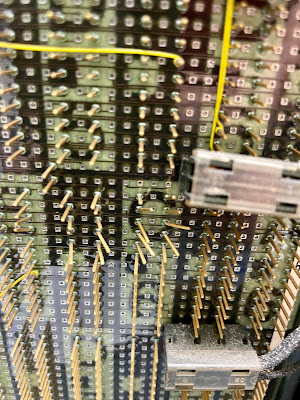
I had not been doing any debugging or signal tracing in A-B1 yet, so I didn't look to closely at it. However, today the light was just right and made these bent pins very obvious to me. Fortunately none are touching each other and none are snapped off, but there may be failure of traces at those locations which I will eventually come across. 


This area is exposed on the rear of the machine and likely was struck by something during transport. I can't imagine any other way this could have occurred. The object was narrow and forced them to the right, some up and some down. 

SHIFTED CHARACTER VALIDATION

I ran through my test loop and typed every possible shifted character. All produced the proper Hollerith code in bits 0 to 12, representing rows 12, 11, then 0 through 9 of a card, in order from left to right. This proves out the health of the contacts in the keyboard, which is a complicated mix of electrical and mechanical encoding. 

Monday, June 13, 2022

Backplane apparent issue was a loose cable!

USING MY DATABASE ENTRIES I TRACED OUT THE CONNECTIVITY OF SIGNALS

With the database containing my captured signal connections, I was able to spit out the list of connections that must exist across compartments and begin some signal testing. The signal did make it from the output of the Program Load latch in gate A, compartment C1 to the edge connector in slot N4. When I moved the other end of my VOM to the destination in gate B, compartment A1 where the other end of the cable is connected, there was no signal at all!

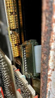
I was pretty sure that I didn't have a failure in the cable itself, so I opened up compartment C1 to look more closely. At once, I saw that the cable had popped out of the slot and was disconnected! The cable itself was in a position where this could happen when gate B snagged on the folded cable coming out of gate A.

I am so relieved that I don't have cascading failures from overly fragile PCBs in the compartments. I will come back after lunch and resume debugging the current problem, failure of the keyboard device controller to reset its interrupt level trigger.

The culprit - loose cable

Yes, I find the rusted out metal edges disgusting too and will deal with them once the system is running well. Likely I will get them to somewhere to be sandblasted and powder coated, or at least sand blasted to remove the corrosion. 

Installed SQL Server, imported signals into database, preparing for my debugging session today

DOWNLOADED MS SQL SERVER DEVELOPER EDITION

Microsoft provides a free license for non-production uses of SQL Server, thus I downloaded and installed the database on my laptop. I also installed the SQL Server Management tool to issue queries to the database.

IMPORTED MY SIGNALS SPREADSHEET TO CREATE A DATABASE

It was easy to export a CSV format file from the spreadsheet, which was importable into my new database. It found the columns and loaded all the entries. I listed it all and was satisfied with the result. Also checked that I could pull up entries with some SQL statements. 

LISTED SIGNALS OF INTEREST FOR MY CURRENT DEBUGGING FOCUS

I listed all the connections for the signals of interest causing the failure with the Run and stop logic of the machine. I also printed a signal I want to check involved in the reset of the Keyboard request for an interrupt, since that problem remains outstanding.

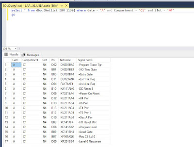
Finally, since I had one failure in connectivity between an edge connector (slot N4 in Compartment C1 of gate A), I listed all the signals connecting to that slot, for a bit of investigation to other possible trace failures going to that slot. 

Listing signals on a given edge connector slot

More backplane failure issues - sigh

SWAPPED CARD FOR THE KEYBOARD CONTROLLER BUT MACHINE FAILED

I had spares of the simple SLT card that implemented the three latches - Keyboard Response, Manual Interrupt and Keyboard select. I had pulled the suspect card to do some bench testing, but I thought I would stick in a spare just to see quickly whether this was indeed a card fault or something off card.

When I turned on the machine, the Run lamp came on except when in Single Step mode, the same symptom that the machine had initially. The one that was caused by a failed trace on a backplane which I jumpered over with wire-wrap. This was triggered at the end of the failure chain by the signal -Prog Ld Not SRP or PT Resp

This signal is forced to low (active) during a program load until the peripheral being booted ends the process. If paper tape is used, the PT Response is activated, while SRP response is from a card reader if that is the boot device. This forces the CPU to run until the boot data is entered into memory.

BEGAN TRACING SIGNALS THAT ARE INVOLVED IN THE ERROR - MULTIPLE ARE OPEN

I found the AND gate that activates the signal, then looked at its inputs which are, not surprisingly, +Program Load, -PT Response and -Level 0 Response (reader end of card interrupt). The levels of the inputs were floating, not a valid 1 or 0 but high enough that the AND gate was triggered. 

This tells me I have connectivity faults between the source of these signals and this gate, once again, I suspect that the simple act of unplugging and replugging a card was enough to worsen hidden cracking in the the backplane PCB. 

THIS IS WHY I PREPARED THE DATABASE BUT IT WILL BE A SLOW PROCESS

With the database, I have the entire route and connectivity of every signal on the system that crosses from ALD pages to others. I am missing some signals that run solely on one backplane between card pins and are only involved in one or two ALD pages but I definitely have every signal that transits from one backplane to another. 

First up is to trace all the signals involved in this latest manifest fault, correct those issues and verify that the system is back to normal operation. My suspicion is that that the cracks are near edges, as that would be where the flex was most when cards were pushed in or pulled out, but I don't know for sure. The two faults I found and corrected were both between edge connectors and an interior card. 

If I have a fault in an edge connector, I can produce a list of all the signals running to a given connector, then trace out the full connectivity for each on the backplane. A sort to give me all the signals by card slot (edge connector), then sort back by signal and look at all the paths for those identified signals. A database sure would be handy here, rather than sorting a spreadsheet, writing down signal names, resorting the spreadsheet and then looking up each signal for its paths. 

Sunday, June 12, 2022

Looking at possible failure in flip flop circuit on SLT card -

TESTED THE CIRCUIT TO RESET THE KBD RESPONSE FLIPFLOP

I monitored the various signals that should trigger the reset of the KBD Response flipflop. These are XIO Sense with Reset 15 AND with Area 1, to form a trigger pulse. That is, when we are doing the sense reset to our device, it drops low. The flipflop reset gate will respond to this falling edge only if the two gating inputs are low. 

One gating input is the value of notQ, thus it is low when the KBD Response flipflop is set. The other gating input is B Bit 1, the sense device value when KBD Response is set in the DSW. The addition of the B Bit 1 as a gate will only reset for this condition as it conditions the trigger for reset. 

I saw the conditions arise that should cause a reset, but it did not change the flipflop. That is why the KBD Response status stays active once it is every triggered and thus continually requests Interrupt Level 4. I will go probe further to see why this is not resetting as it should. I also will pull the card and test it on the bench. 

I captured a good shot of the flipflop being activated. When the keyboard is first pressed, it fires two single shot pulses. One sets a gate for KBD Response then when the second expires we get a falling edge that is the trigger for the flipflop set circuit. You can see the falling edge in dark blue on the oscilloscope, with the purple gating single active (low). The result is shown in the yellow (KBD Response Q output) and cyan (KBD Response notQ output). 

Setting the KBD Response flipflop

Digging into failure to reset request for interrupt

PLAN OF ATTACK TO RESOLVE THE FAILURE TO STOP RETRIGGERING IL4

The circuitry has a flipflop called KB Response that is set when a key is pressed and it is reset when a XIO Sense with Reset Bit 15 is received for Area 1, the device code for the keyboard and console printer. The AND gate in the reset path below is triggered when the KB Resp flipflop is set, so that the notQ output is low, and a pulse arrives from the bottom left AND gate when XIO Sense Reset 15 and Area 1 are both true. 

Logic that resets the keyboard trigger to request IL4

I will monitor the KB Resp line as well as the XIO Sense Reset and Area 1 signals with the oscilloscope. If the XIO and Area 1 lines are true, but the FF doesn't reset, then the issue is on the SLT card itself with the flipflop circuitry. If the lines don't change appropriately the issue is somewhere before the left lower AND gate. 

I hope to discover what is going wrong. Most likely one of the signals is  not getting to the AND gate which resets the response flipflop, but we shall see. It could also be a hot signal setting the flipflop repeatedly, but one that is only becoming hot after the first keypress is registered.