READY TO GET THE FPGA WORKING IN THE VIRTUAL 2315 CARTRIDGE FACILITY
The RK-05 Emulator from George Wiley, which is the basis for my Virtual 2315 Cartridge Facility, has an FPGA, a Raspberry Pi Pico and SDRAM that work together to emulate a disk drive, using data from a file on a microSD card to serve to the disk controller.
I redesigned the emulator to form my virtual cartridge facility. My code is a significant modification of George's, to accommodate the differences between the IBM 13SD disk drive and the DEC RK-05 drive, as well as to implement the unique hybrid mode of operation of my facility. A real disk drive, with a cartridge installed, will spin up and run.
The virtual cartridge facility interposes between the 13SD disk drive and the controller logic in the IBM 1130 computer. The drive arm moves in and out as the controller operates the drive, but the data stream to and from the controller comes from my facility, based on the file in the microSD card. This gives the operator of the computer the sounds and movements from the real disk drive, but avoids disk heads riding on the real disk cartridge. This is valuable as the disk cartridges are precious and the disk heads are basically unobtainium.
LATTICE PROGRAMMER CONNECTED TO DOWNLOAD BITSTREAM
The FPGA chip is a Lattice ICE40HX1K chip. Using the IceCube2 software toolchain, I synthesized my code and produced a bitstream to be loaded into the chip. The Lattice HW-USBN-2B programmer arrived Friday afternoon; it is hooked to the JTAG programmer connector on the RK-05 Emulator box and its software connects to and updates the ROM holding the FPGA code. The flash RAM is an N25Q032A13ESC40F device that is wired to the JTAG interface, providing 32Mbit storage that is used to initialize the FPGA.
TESTING BEGINS WITH PAIRED CODE IN FPGA AND PICO
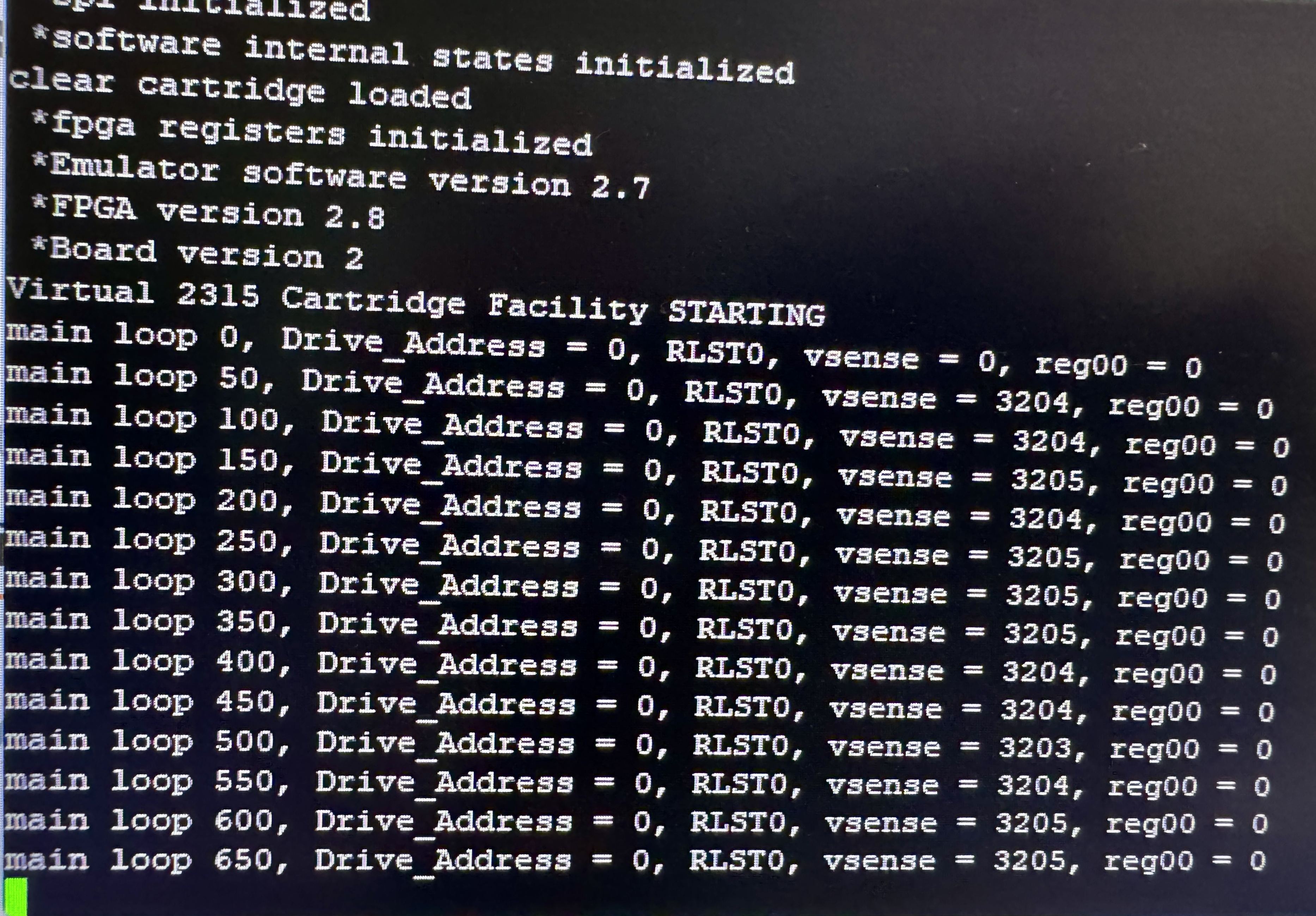
I brought up the box and repeated the testing I had done with the Pico code previously. That is, I had it load a virtual cartridge image from the microSD card, pushing the data down to the SDRAM using the FPGA. The inputs that would come from the disk drive and the disk controller logic are sensed as logically low, since they are not currently connected.
This default asserted that the disk drive was ready to be accessed, allowing the Virtual 2315 Cartridge Facility to show the Ready lamp. However, another signal asserted that a fault occurred in the disk drive, rendering it unsafe to use. The Fault lamp lit on the screen. However, I couldn't unload the virtual cartridge because that requires the File Ready to turn off by going high, which won't happen with the default input state.
My prior tests used the unmodified code from George's emulator, as the data download/upload function didn't change. It showed that the data from the virtual cartridge image was downloaded and when uploaded was a match, both to what was downloaded and to what was on the virtual cartridge file.
My future testing will simulate signals from the 1130 and watch the results to see if it appears to be correct. I can then watch the unload and verify that the virtual cartridge file is still correct. The real testing will take place on the IBM 1130 soon.