1053 CONSOLE PRINTER - SELECTRIC - RESTORATION
I worked the broken end of the old hand cycle tool out of the cycle shaft, then threaded on my newly acquired hand cycle wheel with the degree markings. I used one spring hook I had from an ebay auction to clear out the hole into which the cycle clutch latch spring fits. Now it is just a matter of hooking the spring through that hole deep in the mechanism, then pulling the other end out and affixing it to the cycle clutch lever.
I still have one or more of the pivots, arms, latches or other parts involved in tab operation bound up with congealed lubricant, because when I crank the carrier moves smoothly forward at a fast pace. I will carefully work through the entire chain of parts involved in this, exercising them to free up motion, until the tab operation stops.
As soon as my full set of spring hooks and other tools arrived, I used them to deal with that spring that needed reattachment. These will also help me with the IO selectric mechanism I got from the Itel/Dura word processor - which when restored can operate as a 2741 substitute to deliver an improved 1130 APL operation.
The tab operation was ended by working out the lube, but the unit is currently taking continual print cycles although without a tilt or rotation to a specific character. This may be an adjustment problem since I had removed and reattached part of the cycle clutch mechanism.
OTHER ACTIVITIES
My return from the business trip was quite a bit longer than expected, due to delayed flights, missed connections and extra connections that got me home after 2AM, with a full day of calls booked starting at 8AM later that day. Between lack of sleep, a cold I caught and limited time, I didn't get anything beyond the 1053 work done.
Tomorrow I will spend the morning at the Computer History Museum bringing up the two 1401 machines for an education program and a public demo, since they were short handed. By the afternoon I should be back to the machine, making progress on several fronts.
Saturday, October 11, 2014

Thursday, October 9, 2014
Design work on new keypunch interface and on the interface of peripherals through the 1131 SAC
KEYPUNCH INTERFACE UNIT DEVELOPMENT
I began coding the Keypunch Interface code, although hampered because I didn't have the documentation of the pins I wired to the various signals. It did give me a chance to work out a draft protocol for users of the interface. Design objectives included the use of straightforward ASCII messages that would allow people using terminal programs to operate and test the interface.
With the lack of frames or other demarcations in a serial stream, the protocol had to allow unambiguous recognition of each message or command. Further, we didn't want to use any characters or codes that weren't sure to be available with any terminal program or connection. Marking the start and/or end of a message using only commonly available characters means that we can have that delimiter character also appear as valid data within a message. Thus, we needed a means to 'escape' the delimiter, blocking its special role to frame messages.
I was guided by the conversion table already in use at Computer History Museum to punch hollerith coded BCD characters. Since the 1401 encoding uses fewer characters than seven bit ASCII, only a subset of ASCII characters are in the table. I had the unused characters to choose among.
I somewhat arbitrarily selected the underscore ( _ ) to be the indicator of the start of a message. It would also be the escape character to use when the underscore is valid data - pairs of _ in a row are interpreted as a single data value of _ while an unmatched underscore is the start of a message.
Messages begin with _ and have a 'verb' immediately after the underscore. The message ends with the next unpaired underscore. The interface will detect error conditions such as a card punch message which has more than 80 columns of card data before the next message is recognized.
Some of the verbs are session or control functions, while others are used to punch each card or read another card. _P is followed by up to 80 columns of data and a newline to release the card. _R has no required additional content and will return the content of the next card to move through the 'dup' station of the keypunch.
The format of the data being punched or written is determined by a session state, the mode, which is changed by the verb _MODE and one of the choices ASCII, BINARY or USERTABLE. We have defined a standard or default correspondence between ASCII and Hollerith code. The binary mode we defined sends sets of four ASCII characters representing hexadecimal values, where three of the hex characters cover the twelve rows in which we can place a punch while the first or high order hex value supports release and other control characters. The user table is defined to encode a set of the twelve holes for each of the 128 valid ASCII characters.
_LOAD followed by 512 characters which are valid hex values will load the user table. Each group of four hex characters is used to determine the holes to punch or keypunch functions to actuate for a specific ASCII character. The first group of four encodes character 000 and the last group encodes character 128 (decimal).
When punching cards in the binary mode, if the characters sent are not 0-9 or a-f, a valid hexadecimal digit, an error is detected. Similarly, during the loading of the user table, any character that is not a valid hex digit will trigger an error. Finally, our default ASCII encoding will flag an error for any character that does not have a translation to a set of holes - the first of the four hex digits in the table has a value that indicates the character is an invalid character to punch.
If a newline ASCII character is in the stream of characters being punched, or the user table entry or four hex digits in binary mode specific a release, the release key of the keypunch is activated to feed the next card in position to punch a new card. It is a way of speeding up punching of cards once all the remaining columns of the card will contain blanks.
The verb _VERIFY has either ON or OFF as a valid operand. It determines whether the keypunch interface will save each punched card image and verify it when that card moves through the 'dup' station as the following card is being punched.
The interface will automatically detect when more than three holes are to be punched in one column, using the multipunch key function of the keypunch to ensure that no more than three rows are punched at any time, continuing until all the intended holes have been perforated.
The verb _CLEAR with no required additional text will activate the clear switch on the keypunch to eject all the cards in the various stations. Typically this would be done to end a punch job.
The _R read verb will space the card in the punch station which causes the preceding card to move through the 'dup' station and be sensed in the same columns. As a necessity, any deck of cards to be read must have an extra card at the end which is not read but will be used to drive reading the final data card.
The verb_R to read a card must space 80 times to pass all the columns through the sense station, Thus, when verifying with _VERIFY ON, we must be able to sense up to the last non-blank column of the card in the 'dup' station, even if the card simultaneously being punched has fewer columns and issued a release. We punch characters or spaces up to the larger of the nonblank length of the prior card or the content of the current card, to ensure that both punching and reading for verification act on all required columns.
The serial stream is 9600 baud, 8 bit, no parity, one stop bit, wired in DCE mode, full duplex and uses XON/XOFF for flow control. Note that this excludes the use of the ASCII characters XON and XOFF in any user table. Attempting to load those two positions of the table with any value except a special 'ignore' code will trigger an error.
The interface will respond with ASCII text messages to every command - both errors and a clear confirmation of the verb it received and the action undertaken. For the _R read verb, the content of the card is returned in ASCII, eighty columns terminated with a new line, when the mode is ASCII. For the user table or binary modes, 320 hex digits are returned as groups of four separated by a space, ending with an new line.
IO DEVICE INTERFACE TO 1130 USING SAC
As I continued to build out the logic design for the multiplexing interface to the storage access channel, I found myself with two directions I can take for handling interrupt requests from my attached devices. I can enforce prioritization or I can push some of the control over priority to the software for the various devices and interrupt subroutines.
I can gate the requests and the recognition of XIO Sense ILSW commands to ensure that the higher priority device on my multiplexer triggers interrupts and is serviced first by software. If more than one device on a level has conditions that request an interrupt, I would effectively poll those devices in priority sequence, selecting the top device which had a request.
Only that device's signals would be gated to the SAC. It would cause the interrupt, only that device would return a bit in the ILSW and only that device would know that the interrupt level was active. When that device's request for interrupt service dropped (the conditions were reset by an XIO Sense Device reset bit), I would poll again and pick the next highest device seeking interrupt service.
That has the downside that the interrupt handler would only see the one device at a time, not bits from all interrupting devices on the same level. The handler would be iteratively entered as each device cleared its request and we switched to another needy device. It is possible that an interrupt routine could be written that would do something special when a combination of devices were ready, different from when they sequentially request interrupts; theoretically although I don't know of any 1130 device whose software does this.
The other route I can take is to present the interrupt status and XIO Sense ILSW to all devices simultaneously, depending on the software and my assignment of bit positions in the ILSW to determine the order of servicing within a level. If more than one device on the level has interrupt requests, the XIO Sense ILSW will see all the relevant bits at once. The software will have to decide the order in which these are handled. It may be based on bit position in the ILSW, e.g. left to right as a priority scheme, or some other method.
It is possible that the interrupt routine could set flags for all the affected devices such that they would all be handled after the interrupt exit - one pass through the interrupt routine instead of multiple. If more than one configured device on an 1130 uses the same interrupt level, the IBM designed adapters use the second method, presenting all of the bits to the XIO Sense ILSW and dumping the priority issue on the coder of the software.
The uncontrolled method as used by IBM designed adapter logic is probably the purer route to take, but the 1133 Multiplexer and its support of strings of 2310 or 2311 disk drives might use the first method I posited. I have no documentation on the 1133 with which to determine that question. For the time being, I will design to the uncontrolled model.
I began coding the Keypunch Interface code, although hampered because I didn't have the documentation of the pins I wired to the various signals. It did give me a chance to work out a draft protocol for users of the interface. Design objectives included the use of straightforward ASCII messages that would allow people using terminal programs to operate and test the interface.
With the lack of frames or other demarcations in a serial stream, the protocol had to allow unambiguous recognition of each message or command. Further, we didn't want to use any characters or codes that weren't sure to be available with any terminal program or connection. Marking the start and/or end of a message using only commonly available characters means that we can have that delimiter character also appear as valid data within a message. Thus, we needed a means to 'escape' the delimiter, blocking its special role to frame messages.
I was guided by the conversion table already in use at Computer History Museum to punch hollerith coded BCD characters. Since the 1401 encoding uses fewer characters than seven bit ASCII, only a subset of ASCII characters are in the table. I had the unused characters to choose among.
I somewhat arbitrarily selected the underscore ( _ ) to be the indicator of the start of a message. It would also be the escape character to use when the underscore is valid data - pairs of _ in a row are interpreted as a single data value of _ while an unmatched underscore is the start of a message.
Messages begin with _ and have a 'verb' immediately after the underscore. The message ends with the next unpaired underscore. The interface will detect error conditions such as a card punch message which has more than 80 columns of card data before the next message is recognized.
Some of the verbs are session or control functions, while others are used to punch each card or read another card. _P is followed by up to 80 columns of data and a newline to release the card. _R has no required additional content and will return the content of the next card to move through the 'dup' station of the keypunch.
The format of the data being punched or written is determined by a session state, the mode, which is changed by the verb _MODE and one of the choices ASCII, BINARY or USERTABLE. We have defined a standard or default correspondence between ASCII and Hollerith code. The binary mode we defined sends sets of four ASCII characters representing hexadecimal values, where three of the hex characters cover the twelve rows in which we can place a punch while the first or high order hex value supports release and other control characters. The user table is defined to encode a set of the twelve holes for each of the 128 valid ASCII characters.
_LOAD followed by 512 characters which are valid hex values will load the user table. Each group of four hex characters is used to determine the holes to punch or keypunch functions to actuate for a specific ASCII character. The first group of four encodes character 000 and the last group encodes character 128 (decimal).
When punching cards in the binary mode, if the characters sent are not 0-9 or a-f, a valid hexadecimal digit, an error is detected. Similarly, during the loading of the user table, any character that is not a valid hex digit will trigger an error. Finally, our default ASCII encoding will flag an error for any character that does not have a translation to a set of holes - the first of the four hex digits in the table has a value that indicates the character is an invalid character to punch.
If a newline ASCII character is in the stream of characters being punched, or the user table entry or four hex digits in binary mode specific a release, the release key of the keypunch is activated to feed the next card in position to punch a new card. It is a way of speeding up punching of cards once all the remaining columns of the card will contain blanks.
The verb _VERIFY has either ON or OFF as a valid operand. It determines whether the keypunch interface will save each punched card image and verify it when that card moves through the 'dup' station as the following card is being punched.
The interface will automatically detect when more than three holes are to be punched in one column, using the multipunch key function of the keypunch to ensure that no more than three rows are punched at any time, continuing until all the intended holes have been perforated.
The verb _CLEAR with no required additional text will activate the clear switch on the keypunch to eject all the cards in the various stations. Typically this would be done to end a punch job.
The _R read verb will space the card in the punch station which causes the preceding card to move through the 'dup' station and be sensed in the same columns. As a necessity, any deck of cards to be read must have an extra card at the end which is not read but will be used to drive reading the final data card.
The verb_R to read a card must space 80 times to pass all the columns through the sense station, Thus, when verifying with _VERIFY ON, we must be able to sense up to the last non-blank column of the card in the 'dup' station, even if the card simultaneously being punched has fewer columns and issued a release. We punch characters or spaces up to the larger of the nonblank length of the prior card or the content of the current card, to ensure that both punching and reading for verification act on all required columns.
The serial stream is 9600 baud, 8 bit, no parity, one stop bit, wired in DCE mode, full duplex and uses XON/XOFF for flow control. Note that this excludes the use of the ASCII characters XON and XOFF in any user table. Attempting to load those two positions of the table with any value except a special 'ignore' code will trigger an error.
The interface will respond with ASCII text messages to every command - both errors and a clear confirmation of the verb it received and the action undertaken. For the _R read verb, the content of the card is returned in ASCII, eighty columns terminated with a new line, when the mode is ASCII. For the user table or binary modes, 320 hex digits are returned as groups of four separated by a space, ending with an new line.
IO DEVICE INTERFACE TO 1130 USING SAC
As I continued to build out the logic design for the multiplexing interface to the storage access channel, I found myself with two directions I can take for handling interrupt requests from my attached devices. I can enforce prioritization or I can push some of the control over priority to the software for the various devices and interrupt subroutines.
I can gate the requests and the recognition of XIO Sense ILSW commands to ensure that the higher priority device on my multiplexer triggers interrupts and is serviced first by software. If more than one device on a level has conditions that request an interrupt, I would effectively poll those devices in priority sequence, selecting the top device which had a request.
Only that device's signals would be gated to the SAC. It would cause the interrupt, only that device would return a bit in the ILSW and only that device would know that the interrupt level was active. When that device's request for interrupt service dropped (the conditions were reset by an XIO Sense Device reset bit), I would poll again and pick the next highest device seeking interrupt service.
That has the downside that the interrupt handler would only see the one device at a time, not bits from all interrupting devices on the same level. The handler would be iteratively entered as each device cleared its request and we switched to another needy device. It is possible that an interrupt routine could be written that would do something special when a combination of devices were ready, different from when they sequentially request interrupts; theoretically although I don't know of any 1130 device whose software does this.
The other route I can take is to present the interrupt status and XIO Sense ILSW to all devices simultaneously, depending on the software and my assignment of bit positions in the ILSW to determine the order of servicing within a level. If more than one device on the level has interrupt requests, the XIO Sense ILSW will see all the relevant bits at once. The software will have to decide the order in which these are handled. It may be based on bit position in the ILSW, e.g. left to right as a priority scheme, or some other method.
It is possible that the interrupt routine could set flags for all the affected devices such that they would all be handled after the interrupt exit - one pass through the interrupt routine instead of multiple. If more than one configured device on an 1130 uses the same interrupt level, the IBM designed adapters use the second method, presenting all of the bits to the XIO Sense ILSW and dumping the priority issue on the coder of the software.
The uncontrolled method as used by IBM designed adapter logic is probably the purer route to take, but the 1133 Multiplexer and its support of strings of 2310 or 2311 disk drives might use the first method I posited. I have no documentation on the 1133 with which to determine that question. For the time being, I will design to the uncontrolled model.
Tuesday, October 7, 2014
Tools to work on 1053 console printer of the 1130 - Selectric tools
I have been fortunate to find quite a few tools that are designed for servicing Selectric mechanisms, most of which make tasks on the printer much easier to do. The first group came from a mislabeled eBay auction - it was a bunch of parts and tools labeled as vintage mainframe parts. The second was an offer by a retired service person who offered to sell some specialized tools he had.
The eBay lot was obviously IBM typewriter parts but had some tools included. When I looked closer, I saw that there was a degree wheel for hand cycling, a cclip holer, t handle and other tools that are ideal for certain assembly steps where it is nearly impossible to get fingers or standard tools in place. Because of the miscategorization, it sold for $9.95 with free shipping.
The retired service person has other tools that will be incredibly handy, particularly the spring hooks which I can use to attach the pesky spring for the cycle clutch latch. One of them will hold a spring at the end of a rod, allowing you to maneuver the end of the spring into its hole, but remains attached to the spring until you release it. This means I can grasp the closer end of the spring with a spring hook, pull it into its attachment location, before releasing the far end of the spring deep inside the machinery.
 |
| Lot on ebay mislabeled as vintage mainframe parts |
The retired service person has other tools that will be incredibly handy, particularly the spring hooks which I can use to attach the pesky spring for the cycle clutch latch. One of them will hold a spring at the end of a rod, allowing you to maneuver the end of the spring into its hole, but remains attached to the spring until you release it. This means I can grasp the closer end of the spring with a spring hook, pull it into its attachment location, before releasing the far end of the spring deep inside the machinery.
 |
| Spring hooks to attach teeny springs in nearly inaccessible locations |
Design work on interface to hook devices to 1130 through SAC
DESIGNING 1130 SAC INTERFACE BOX
One of my objectives in designing the interface to hook up peripherals to the 1130 was to allow more than one device to be hooked up at the same time. Outbound access from the 1131, via the XIO instructions, is inherently serialized but inbound access, both cycle stealing to move data and requests for interrupts, may occur from more than one of the devices in uncontrolled sequences.
Interrupt levels could be used by more than one device on my box, thus I have to keep track of requests and present them in appropriate priority order. Cycle steal requests share a single level with the SAC, but if more than one device asks for cycle stealing, I not only have to keep track and present requests in some order. I also have to block the devices which are not given the cycle stealing hardware from seeing the CS level occur.
The logic for each device would presume that when CS level 1 is active, its request for cycle stealing was granted. All devices which requested cycle stealing will attempt to control the hardware when they see CS Level 1 active.
I realized that on the 1130 system, the SAC is designed to support just one connected device. In order to handle more than one, the 1133 Multiplexer cabinet is hooked to the SAC. The multiplexing logic in the 1133 is similar to what I want to do - it divides up the devices into a number of multiplex levels, prioritizing access, blocking visibility of control signals and holding requests until they can be presented.
I have a general outline for how I will implement the multiplexing, working from the control lines that are available on the SAC, the outbound sequences for XIO instructions and some thinking about the conditions and states that can exist for inbound requests from the devices.
Since each device adapter is responsible for almost all of the work of tracking the XIO instruction, latching data, signaling for writes to core, handling interrupts, cycle steals and sense status, the multiplexer logic is only involved in gating the interrupt and cycle steal signals between devices and the 1131. It only has to switch the gating based on priority as the active device drops its requests.
I also have a design for the FSM to track the stages of an XIO instruction and to recognize when to take certain actions such as latching data from the 1131, setting up and signaling channel write for data going out to the 1131, and setting other status information. This is the logic needed at the heart of a device adapter. It can be instantiated for each device interface being implemented for connection through the SAC.
One of my objectives in designing the interface to hook up peripherals to the 1130 was to allow more than one device to be hooked up at the same time. Outbound access from the 1131, via the XIO instructions, is inherently serialized but inbound access, both cycle stealing to move data and requests for interrupts, may occur from more than one of the devices in uncontrolled sequences.
Interrupt levels could be used by more than one device on my box, thus I have to keep track of requests and present them in appropriate priority order. Cycle steal requests share a single level with the SAC, but if more than one device asks for cycle stealing, I not only have to keep track and present requests in some order. I also have to block the devices which are not given the cycle stealing hardware from seeing the CS level occur.
The logic for each device would presume that when CS level 1 is active, its request for cycle stealing was granted. All devices which requested cycle stealing will attempt to control the hardware when they see CS Level 1 active.
I realized that on the 1130 system, the SAC is designed to support just one connected device. In order to handle more than one, the 1133 Multiplexer cabinet is hooked to the SAC. The multiplexing logic in the 1133 is similar to what I want to do - it divides up the devices into a number of multiplex levels, prioritizing access, blocking visibility of control signals and holding requests until they can be presented.
 |
| Role of 1133 as a multiplexer for more than one device through SAC |
Since each device adapter is responsible for almost all of the work of tracking the XIO instruction, latching data, signaling for writes to core, handling interrupts, cycle steals and sense status, the multiplexer logic is only involved in gating the interrupt and cycle steal signals between devices and the 1131. It only has to switch the gating based on priority as the active device drops its requests.
I also have a design for the FSM to track the stages of an XIO instruction and to recognize when to take certain actions such as latching data from the 1131, setting up and signaling channel write for data going out to the 1131, and setting other status information. This is the logic needed at the heart of a device adapter. It can be instantiated for each device interface being implemented for connection through the SAC.
Friday, October 3, 2014
The circuits - TTL to SLT interfaces to 1130 SAC transmission lines (signal cables)
DRIVER CIRCUIT
Here is the driver circuit which takes TTL inputs and drives the twisted pair transmission lines used in 1130 signal cables, particularly the Storage Access Channel. It is shown with the circuitry of the 5807916 receiver card that is used with the SAC.
RECEIVER CIRCUIT
Here is the receiver circuit which terminates the twisted pair transmission lines used in 1130 signal cables, particularly the Storage Access Channel, and yields a TTL level signal. It is shown with the circuitry of the 5803447 driver card that is used with the SAC.
Here is the driver circuit which takes TTL inputs and drives the twisted pair transmission lines used in 1130 signal cables, particularly the Storage Access Channel. It is shown with the circuitry of the 5807916 receiver card that is used with the SAC.
 |
| My driver circuit on left to interface TTL to 1130 SAC cable |
RECEIVER CIRCUIT
Here is the receiver circuit which terminates the twisted pair transmission lines used in 1130 signal cables, particularly the Storage Access Channel, and yields a TTL level signal. It is shown with the circuitry of the 5803447 driver card that is used with the SAC.
 |
| My circuit on right to detect 1130 SAC signals as TTL level logic outputs |
Thursday, October 2, 2014
Working on receiver and driver circuits to interface to 1131 SAC
DRIVER CIRCUIT
The driver is quite easy, as it is a transistor that will pull the transmission line down to ground or let it float up to the +3V supplied through the far end's 95 ohm pull up resistor/terminator. Doesn't require simulation and testing.
1131 SAC TRANSMISSION LINE BEHAVIOR
The transmission line is twisted pairs with 93 ohm characteristic impedance, allowed to have up to 33 ohms resistance, with a 95 ohm terminator resistor pulling the receiver end up to +3V. The driver is a transistor that will pull the line down to ground or let if float up.
The challenge is dealing with the maximum resistance case - 33 ohms - as that produces an off state at over .75 volt, well above the SLT specification of .3V max for a logic level 0. The logic 1 case, +3V is well above the minimum of 1.8V and quite satisfactory, even with a bit of loading from a receiver circuit it will meet specs.
RECEIVER CIRCUIT
I have to design a receiver that will properly yield a logic 0 when the line is above .75V, and generate a logic 1 when the voltage is up close to 3V. If I simply hooked up a standard logic gate to the transmission line, the gate must interpret the .75-.8 volt level as a fully legal binary 0.
I am working on discrete components as a receiver circuit, allowing me to control the behavior and simulate it as I tweak the design. Unless I figure out a standard gate that is sure to interpret my levels properly, the custom design is necessary.
The driver is quite easy, as it is a transistor that will pull the transmission line down to ground or let it float up to the +3V supplied through the far end's 95 ohm pull up resistor/terminator. Doesn't require simulation and testing.
1131 SAC TRANSMISSION LINE BEHAVIOR
The transmission line is twisted pairs with 93 ohm characteristic impedance, allowed to have up to 33 ohms resistance, with a 95 ohm terminator resistor pulling the receiver end up to +3V. The driver is a transistor that will pull the line down to ground or let if float up.
The challenge is dealing with the maximum resistance case - 33 ohms - as that produces an off state at over .75 volt, well above the SLT specification of .3V max for a logic level 0. The logic 1 case, +3V is well above the minimum of 1.8V and quite satisfactory, even with a bit of loading from a receiver circuit it will meet specs.
RECEIVER CIRCUIT
I have to design a receiver that will properly yield a logic 0 when the line is above .75V, and generate a logic 1 when the voltage is up close to 3V. If I simply hooked up a standard logic gate to the transmission line, the gate must interpret the .75-.8 volt level as a fully legal binary 0.
I am working on discrete components as a receiver circuit, allowing me to control the behavior and simulate it as I tweak the design. Unless I figure out a standard gate that is sure to interpret my levels properly, the custom design is necessary.
Wednesday, October 1, 2014
Designing interface to use 1130 Storage Access Channel to interface arbitrary modern peripherals to the system
BUILDING SAC INTERFACE TO 1131
I spent some time during my cross country flights developing interface circuits that would take TTL logic levels and drive valid inputs to SLT logic, plus circuits to take SLT inputs and drive TTL logic outputs. These converters will sit between the Storage Access Channel circuitry in the 1130 and whatever logic I build to interface various devices to the 1130.
To do this, I started with the circuits used in the 1130 for sending the SAC signals out and for receiving inbound signals. One of the cards is defined in the online SLT designers documentation on bitsavers.org, but the receiver was not. By carefully studying all the various SLT and card schematic documentation, I was able to reconstruct the receiver card.
The transmission line driver and receiver for the SAC is the 30ns family AI without load resister feeding an AOI on the receiving end, the end of the line terminated by a 95 or 100 ohm pullup resistor to +3V.
The usual transmission receiver card has one input to an AOI (and-or-inverter, the basic logic gate of SLT) so it acts like a NOT gate but restores the logic signal. The driver is an and-inverter with just one input so it too functions as a NOT, but driving more current than a normal logic gate output, and with no pullup resistor on the collector of the inverter.
The receiver in the 1130 SAC uses two inputs in the AOI - acting as an AND gate, with one of the two inputs used to gate whether the incoming bit is passed on to the rest of the 1131. One such input is the 'write gate' that is set when a device is transferring data from a read into memory or during a cycle steal handling a read.
The usual receiver card has ten AOI circuits on board. The board in the 1130 SAC uses nine AOI - one AOI is used to receive the gating control signal, such as channel write gate, this signal then gates the other eight AOI which deliver the gated inbound bits.
Because of all the documentation, I am very confident that I have reconstructed the circuits on both sides. I was able to simulate them, verify the voltages, currents, transition points and other characteristics. This is necessary since my circuits will masquerade as a driver or a receiver, depending on whether a signal in outbound or inbound to the 1131.
Based on this circuit, reception is pretty easy - I hold the line up to 3V with a 95 ohm resistor and sense the voltage. Logical 1 is 1.8V to 3V, while logical 0 is .3V or lower and of course the zone in between is undefined. I am going to design my circuit to produce TTL level signals but also raise an alarm signal if the value is in the forbidden zone. I can use this to troubleshoot electrical and reliability issues.
The driver is even simpler - it is a transistor that will conduct when the intent is to send a logical 0, otherwise it lets the signal float. The 95 ohm terminator resistor on the far end will pull the line to 3V when we have a logical 1, and I will pull about 30ma of current through the transistor to drag the line down to near 0 volts for logical 0. I expect to have only a few millivolts at the far end, the result of wire resistance, transmission line mismatch and inherent resistance in the transistor - this will be well below the 300mv that is the cutoff for a valid logical 0 state.
I also developed all the rules for when I have to assert certain lines or latch in data, to implement the XIO instructions, interrupt handling and cycle stealing functions. It appears quite straightforward to produce a single device that connects to the SAC, although I want to design a more generalized interface that may have multiple devices connected simultaneously.
Over the coming couple of days I will work out the design approach for the generalized interface, allowing several devices to share the device. Whatever fpga board I use to implement this needs 76 I/Os for the SAC cable (36 output and 40 inbound signals), although I can disregard a few of them, e.g. CPU Meter In and Meter Out, since I don't care about running usage meters for billing purposes.
The board then needs additional IOs to attach all the intended devices. This will be a major design and sourcing factor. Most lower cost fpga boards have limited IO pins even if the fpga chip onboard itself has many hundreds of input/output pins - most are not connected externally.
I spent some time during my cross country flights developing interface circuits that would take TTL logic levels and drive valid inputs to SLT logic, plus circuits to take SLT inputs and drive TTL logic outputs. These converters will sit between the Storage Access Channel circuitry in the 1130 and whatever logic I build to interface various devices to the 1130.
To do this, I started with the circuits used in the 1130 for sending the SAC signals out and for receiving inbound signals. One of the cards is defined in the online SLT designers documentation on bitsavers.org, but the receiver was not. By carefully studying all the various SLT and card schematic documentation, I was able to reconstruct the receiver card.
The transmission line driver and receiver for the SAC is the 30ns family AI without load resister feeding an AOI on the receiving end, the end of the line terminated by a 95 or 100 ohm pullup resistor to +3V.
The usual transmission receiver card has one input to an AOI (and-or-inverter, the basic logic gate of SLT) so it acts like a NOT gate but restores the logic signal. The driver is an and-inverter with just one input so it too functions as a NOT, but driving more current than a normal logic gate output, and with no pullup resistor on the collector of the inverter.
The receiver in the 1130 SAC uses two inputs in the AOI - acting as an AND gate, with one of the two inputs used to gate whether the incoming bit is passed on to the rest of the 1131. One such input is the 'write gate' that is set when a device is transferring data from a read into memory or during a cycle steal handling a read.
The usual receiver card has ten AOI circuits on board. The board in the 1130 SAC uses nine AOI - one AOI is used to receive the gating control signal, such as channel write gate, this signal then gates the other eight AOI which deliver the gated inbound bits.
Because of all the documentation, I am very confident that I have reconstructed the circuits on both sides. I was able to simulate them, verify the voltages, currents, transition points and other characteristics. This is necessary since my circuits will masquerade as a driver or a receiver, depending on whether a signal in outbound or inbound to the 1131.
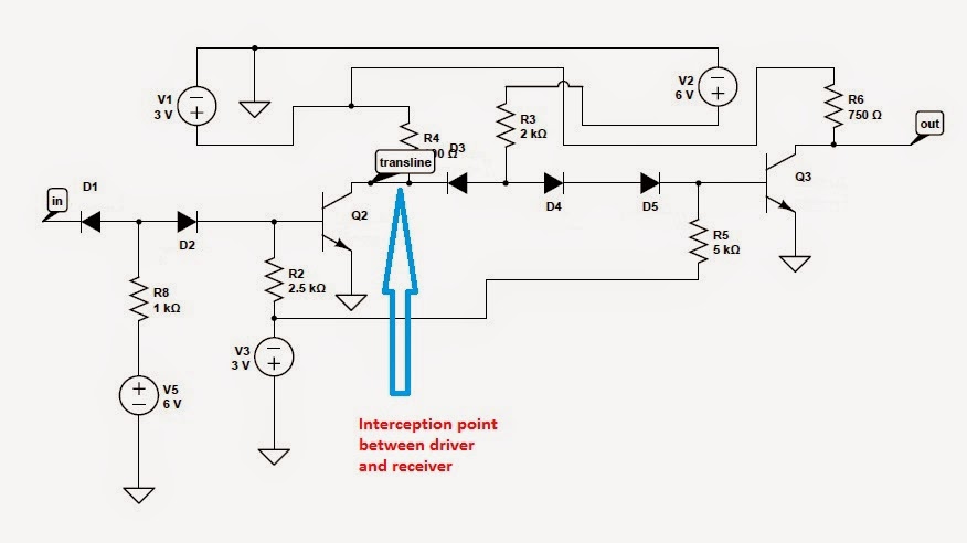 |
| Recreated 1130 SAC driver and receiver circuitry, showing point where my circuits replace left or right side |
The driver is even simpler - it is a transistor that will conduct when the intent is to send a logical 0, otherwise it lets the signal float. The 95 ohm terminator resistor on the far end will pull the line to 3V when we have a logical 1, and I will pull about 30ma of current through the transistor to drag the line down to near 0 volts for logical 0. I expect to have only a few millivolts at the far end, the result of wire resistance, transmission line mismatch and inherent resistance in the transistor - this will be well below the 300mv that is the cutoff for a valid logical 0 state.
I also developed all the rules for when I have to assert certain lines or latch in data, to implement the XIO instructions, interrupt handling and cycle stealing functions. It appears quite straightforward to produce a single device that connects to the SAC, although I want to design a more generalized interface that may have multiple devices connected simultaneously.
Over the coming couple of days I will work out the design approach for the generalized interface, allowing several devices to share the device. Whatever fpga board I use to implement this needs 76 I/Os for the SAC cable (36 output and 40 inbound signals), although I can disregard a few of them, e.g. CPU Meter In and Meter Out, since I don't care about running usage meters for billing purposes.
The board then needs additional IOs to attach all the intended devices. This will be a major design and sourcing factor. Most lower cost fpga boards have limited IO pins even if the fpga chip onboard itself has many hundreds of input/output pins - most are not connected externally.
Subscribe to:
Posts (Atom)