Monday, February 28, 2022

Finished soldering the circuit board for the IBM 1130 Extender

 GOT TO SHOP FOR A FEW HOURS TODAY AND FINISHED ALL THE SOLDERING

A few hundred parts were soldered on today, completing the board itself. I will need to mount it in the case and wire up the connections, but some serious checking and testing should be accomplished first.

Board ready for mounting and connection
One receiver circuit, IBM 1130 output to FPGA input


Sunday, February 27, 2022

IOB6120 parts have all arrived and the PCB is waiting for DHL pickup at the factory

 My shipments from Digikey, Mouser and several eBay vendors have all arrived. I have all the components needed to assemble the unit and have only to wait for the PCB itself to arrive.

The factory has assigned a DHL Express number but not yet handed the box over to the shipper. Once it begins traveling I should get a delivery date, probably towards the end of the week, and can watch it make its way towards me. 

Friday, February 25, 2022

Got a bit more done before relatives arrive for multi day visit, during which no work will get accomplished at shop

PERMANENT INSTALLATION OF 3.0V POWER RAIL COMPONENTS

I installed the voltage regulator and heat sink that powers the +3V side of my receiver circuits. Testing showed it producing exactly the correct voltage at all the delivery points at the receiver circuits. 

FINISH 500 OHM RESISTORS AND INSTALL ALL 12K RESISTORS

I put on the last of the 500 ohm resistors, which couple the receiver circuits to the FPGA input pins. I then installed all of the 12K base pull up resistors for the receiver circuits. Ahead of me are the soldering for all the 100 ohm, 700 ohm, 1.5K ohm and 1K ohm parts that will complete the receiver circuits. 

IOB6120 PCB NEARING COMPLETION

The board is in the process of having the silkscreen printed on, after which it has hot air solder leveling (tinning), electrical testing, and is cut out of the panel for boxing and delivery. The last of my parts for this project should arrive by Monday, ahead of the PCB, although the 1130 Extender box construction will take precedence.

Thursday, February 24, 2022

Assembly day one - ICs, capacitors, power check, transistors installed, beginning on resistors

 POWER SECTION TEST

I soldered on the decoupling and filtering capacitors to the board and then installed the PC power supply connector. After validating correctness of the lines, I plugged in a power supply and it came up with all the proper voltages on the power rails. 

DRIVER INTEGRATED CIRCUITS INSTALLED

The driver circuits for signals going out to the IBM 1130 processor make use of surface mount sized 74LS06 chips, hex open circuit inverters. I soldered these down to the board and inspected the connections.

RECEIVER CIRCUIT TRANSISTORS INSTALLED

The receiver circuits for signals coming from the IBM 1130 are implemented with one transistor and six resistors apiece. I designed this with moderate sized surface mount parts, SOT-23-3 for the transistor and 0805 for the resistors. I soldered the transistors into all 36 circuits.

MECHANICAL FIT TESTING

I checked that the header pins line up properly with the FPGA board. I tested the fit of various connectors, one bringing 24VAC from the 1130 as power sequencing voltage, another two implementing SPI links, and the heat sink clearance for the 3V regulator (since PC powers supplies produce 3.3V, not the 3.0V that is used with SLT logic). 

BEGINNING INSTALLATION OF RESISTORS IN THE RECEIVER CIRCUITS

The output of each receiver circuit is coupled through a 500 ohm resistor to an input pin of the FPGA. I began soldering these resistors on the board and go about 2/3 through it by the time I had to close up shop. 

Wednesday, February 23, 2022

Finally have board and can begin to work on the project

BIG SIGN TAPED TO FRONT DOOR, DHL COURIER FINALLY LEFT PCB PACKAGE

After receiving an error from the DHL website that I had exceeded my quota of delivery change requests as I tried to correct the phone number they put in the notes, I printed a sign for the front door of my building alerting the courier to just leave the package outside that door and call me. 

The customer service line yesterday told me they put my phone number in the notes, but the number there was a long amalgam of the number of JLCPCB.com and my number that would NOT have reached me. Sigh. Since it was more than ten minutes wait for the agent on chat last time, plus pauses while they read the delivery file, I went with a more direct method of communciation.

It worked! The package was left in front of the door as I requested. 

BEEPING OUT CONNECTIONS (JUST BECAUSE IT WOULD BE A PITA TO DESOLDER)

I made sure of a number of connections:

  • No shorts between power lines and ground
  • Continuity of screw terminals to their destinations
  • Lack of shorts of screw terminal lines to power rails or ground
  • Lack of shorts between pins of ICs and pins of FPGA socket
  • Continuity of sources to fpga socket pins
  • Correctness of power rails and ground to fpga and ICs
  • correctness of connections of receiver circuits
  • Correctness of connections of power supply and regulator
  • Correctness of connections for LED signals

TESTING MECHANICAL FIT

I fitted a few screw terminals to be sure that I had access to add and change wires to all the terminals with the relatively dense arrangement on the PCB. Similarly, I tested the fit of connector parts and other components to be sure I didn't get the mechanical layout wrong.


Tuesday, February 22, 2022

My 1130 Extender PCB intended to arrive today (early!) - due to idiocy it may be tomorrow or never

DHL INFORMED ME IT WILL DELIVER THE BOARD EARLY

The PCB, listed as scheduled for delivery on the 24th, was out for delivery today, the 22nd, ahead of the estimated date. It is coming by DHL Express. I set up the delivery to skip signature, asking them to leave it at the door if they don't reach me. 

At 5:09 tonight, while my wife and I were home upstairs, the courier from DHL issued an exception claiming nobody was home and departed with my package. It is a condominium building and if they don't have a code like Fedex, UPS and the post office, they just have to hit the button for our unit and call us.

No ring from the courier. No package left at the door. I am told to go online and reschedule, which sounds like an infinite loop in the making as the dolt will not get in tomorrow, will still be unable to push a button on a directory, and therefore my PCB may never be delivered. 

MEANWHILE THE IOB6120 BOARD PROCEEDS THROUGH MANUFACTURING

They have laminated the sandwich after building the inner layer traces and are drilling the holes. Soon they will lay down copper, plate the vias and begin to etch the copper traces for the top and bottom layers. 

Monday, February 21, 2022

Fabricated back level version of IOB6120 board, need to apply corrections

REVISION B VERSUS REVISION A - BATTERY DRAIN

Apparently it was discovered after the first batch of IOB6120 boards were put into service that the drain on the batteries that provide nonvolatile memory protection was excessive. A change was introduced as revision B which introduced four diodes and pullup resistors that isolated the chip select lines from the TTL drive chips that fed them. 

Instead of having the battery power feed back from the SRAM and Flash to the TTL output pin, a diode isolates the two and a pullup resistor ensures that the chip is not selected until the TTL chip is driving a low output during normal powered operation.

I SENT REV A TO THE FAB, NEED TO RETROFIT FIX

The version of the gerber files I transmitted to the factory were for the original revision A boards. The manual with the bill of materials does not list the diodes and resistors from the revision B, thus I never spotted the discrepancy.

After the problem was found, those with rev A boards wanted to retrofit a fix. The method involves breaking the trace on four select lines from the TTL chip to the various battery powered nonvolatile chips, bridging the broken trace with a small surface mount diode, then tacking on a teeny resistor whose other end is routed to VCC with a jumper wire. 

This is done in four places, for the FPGA select, Flash select, cf select and status select circuits. The devices to place on the board are pretty small and this requires delicate work, which I will probably do prior to populating the PCB with the other components. 

ORDERED RESISTORS AND DIODES

I placed an order with Digikey for 1mm long surface mount diodes, definite overkill with 65V 100 ma ratings. I chose 0603 sized resistors as a compromise between minimizing the risk it will overlap another trace and minimizing the risk that I can't place and solder it due to small size. I felt that 0603 was a reasonably large resistor that would not be too hard to locate somewhere free of interference with other traces. 

Some incompatibilities, appears I can resolve them to use 32M flash in place of 4M flash chip

SUBSTITUTION POSSIBILITY FOR FLASH CHIP ON IOB6120

The IOB6120 was designed to use a Sharp flash memory chip, the LH28F400BHVE-BL85, but that chip is so obsolete that there are not even entries for it with suppliers like Digikey or Mouser. I did find a very limited supply of a newer Sharp flash memory, which is larger but uses the same TSOP 48 pin layout and has almost full pin compatibility. Thus, if I can resolve any conflicts and verify that it should operate properly, I can install this 32Mb flash chip in place of the 4Mb chip in the design.

BYTE MODE USED ON DESIGN CHIP, DOESN'T EXIST ON SUBSTITUTE

The chip used in the design is a 4Mb chip that either addresses 256K 16 bit words or 512K bytes. The substitute does not offer a byte mode, it always returns 16 bit words and thus the 32Mb chip addresses 2M locations versus 256. This uses three additional address bits for the new chip, and on the old chip it needed an extra bit to select the upper or lower byte of a 16 bit word.

ADDRESS BIT OVERLOAD OF Q15 PIN ON DESIGN CHIP

The old chip, for which the IOB6120 is designed, allows selection of the upper or lower byte of a word by using data bit 15 as an input, called the A(-1) address bit. This works in byte mode because the data bits 8 to 15 are floating, not driven, when in byte mode. D15 can be used as an input in that mode.

The substitute chip, however, drives all 16 data bits in output mode, which would conflict with the driven A(-1) signal hooked to D15. This is the biggest conflict in the use of this chip in place of the design part.

POTENTIAL RESOLUTION INVOLVES MINOR REWORK ON BOARD

If I cut the trace delivering the A(-1) address bit to D15, then the output will be driven but have no destination. That is fine since we have plenty of extra words in this larger substitute chip and can afford to only use the bottom 8 bits of each of the 2M words, which is still more than the 512K bytes the design chip addresses.

I would then route the A(-1) bit over to one of the three unused high address pins on the new chip with a jumper wire. Assuming these pins are not grounded through to the inner plane, the only question is where I pick up the A(-1) signal for the jumper over to the address pin such as A20 I would use for my modification.

MAJOR QUESTION ON CUI MODE DIALOG WITH FLASH CHIP AND DATA BIT 15

This device is designed to operate in SRAM compatibility mode for reading - simply supply an address, strobe the appropriate select and output enable control pins, and you are able to read to the chosen address. If the design only uses this mode, then all will be well if I resolve the A(-1) bit address issue as discussed above. 

On the other hand, this chip also needs the Command User Interface (CUI) mode to do writes. CUI sends commands and data to the controller onboard the chip. The 4Mb chip will handle CUI on the low 8 data bit lines when the chip is put in Byte mode, as it was in the IOB6120 design. The 32Mb chip handles CUI over the full 16 bit data width and therefore probably will not work properly with D15 bit floating and commands and data sent only on the low eight bits. 

ALTERNATIVE FOUND AT A HIGHER PRICE 

I did discover a newer Sharp flash chip that supports the byte mode and thus would be fully pin compatible, simply with higher capacity that the chip in the design. It is the LH28F160BJHE-BTLTH also TSOP 44 format and its higher capacity makes use of pins that are N/C on the design chip.  Looking for quotes at a reasonable price but I can pay $20 for four of them on eBay and hope they are not counterfeit. 

Sourcing parts for IOB6120 build, including obsolete and unobtainium components

DIGIKEY AND MOUSER COVERED MOST PARTS I NEEDED

The majority of all the parts are still stocked, either at Digikey where I bought most or at Mouser. That ran to about $120 between the two, including pricy parts such as the FPGA chip. Unfortunately a few were not even on the systems at either vendor or are marked obsolete and not stocked. 

MISSING ITEMS

I didn't have a source for the 4MB flash memory chip, the four SRAM chips, the CF socket and some 085C form factor 10uf polarized capacitors. I can work out a bodge for the capacitor, but the others were more critical to resolve. 

EBAY SOURCED SOME PARTS, THUS SOME RISK OF FAKES

I was able to find the SRAM chips listed on ebay from quite a few vendors. Those in China had a higher risk of being fakes as the industry that manufactures false chips is mainly centered there, but there were two vendors who at least claimed to ship from the US. No guarantee that the devices are any more correct but at least I can set up my Retro Chip Tester Pro to validate the parts before I solder them onto the board. 

The Molex CF socket is very obsolete and not stocked. I found one socket on ebay that superficially looks like the Molex part, but the vendor doesn't provide enough information to tell whether it matches the footprint and pin assignments of the Molex part. I took a gamble since it is not a very high priced item and purchased it.

INVESTIGATING SUBSTITUTION FLASH CHIP WITH EXISTING DESIGN

The part which seems to be pure unobtainium is the Sharp 4MB flash rom, LH28F400BVHE-BL85, that is in a 48 pin TSOP package. The usual suspect sites asking me to submit a request for quote popped up, but nothing looked too trustworthy in any case. I did search for similar chip types online and came up with a very limited supply of a different Sharp 32MB flash rom on Digikey. It was the same package type thus it was time to compare datasheets and pin assignments. 

At first glance, the pin assignments are almost identical and the differences are in most cases where the new chip has no connection to a pin that was wired on the old one. There are three additional address bits, of course, but those pins are not used on the old chip. 

The most serious red flag at first glance is that the missing chip has a BYTE control line that is N/C on the new chip. Thus, if the IOB6120 is trying to read/write in byte mode while the potential substitute is always a 16 bit word operation, we may have a problem. 

I will be scanning the data sheets rigorously, but I did buy the substitute right away since it is limited in quantities. I have to check the protocols, timing and other details carefully to be sure that I can substitute in this larger capacity chip successfully. 

Sunday, February 20, 2022

Teletype restorations partially completed, plus preparing to build two interesting projects

ASR/33 NUMBER ONE - MOSTLY WORKING NOW

David brought his teletypes over to my workshop where we could jointly work on them to get them working properly. He can attach them to his vintage DEC equipment once this happens. Turns out he has multiple units, which greatly increases the chances he can get one or two fully working machines. 

The system he designated number one was given the most attention by us. It took some time to get the keyboard adjusted properly. On a teletype, when you push down a key, it rotate a lever which connects through an H shaped plate to another lever that eventually trips the clutch to fire off one cycle of the distributor. 

The distributor is a parallel to serial converter. The keyboard emits eight signals - bits - which encode an ASCII character. The distributor converts those eight bits into a stream of a start bit, seven data bits, one parity bit and a stop bit. The clutch needs to be tripped for every key press in order to send out that data serially. At the end of the distributor cycle it resets the keyboard so the next key can be depressed. 

The mechanism has to be carefully adjusted so that the clutch is reliably tripped but only once per keypress. That involves moving a bracket carefully with two screwdrivers until the desired behavior ensures. I tweaked this on the keyboard.

However, several things have to happen correctly. The keyboard encoder, a set of wire contacts and levers which make or break the contact with fixed terminals, has to produce the right bit values for the key selected. We used a continuity checker to test this and found that it was not working well. 

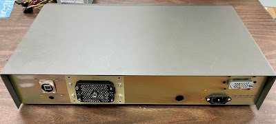
After some tweaking of contacts and adjustment of the position of the terminal block, the parallel data bits from the keyboard were correct. The next step is that the contacts on the distributor have to work properly so that the serial output matches that ASCII character. Fortunately that worked well. With the power supply generating the 20ma current source, we had a teletype that sends keypresses out correctly.

Putting the machine in 'Local' mode will connect the sent data to the receive circuit, ultimately driving the machinery to type characters or perform functions like line feed. In order for that to work properly, many things must perform correctly. The receiver driver board has to drive 48V to the solenoid based on the incoming current (or the looped data from the send circuit). 

The reception clutch sits at the stop position while the current is flowing - a condition called Mark in teletype circuits. As soon as the start bit arrives, a Space condition meaning interrupted current, the clutch is tripped and begins rotating. As each bit arrives serially, the solenoid is either attracted in the Mark condition or loose in the Space condition. That sets up levers in the decoder machinery, one lever for each of the bits arriving. Finally, the stop bit is a Mark and causes the clutch to hit the stop tab and end the reception cycle for that character. 

After the bits are set up, they move a number of long side to side levers which have notches in some locations. Those levers also are connected up to the typehead where they control the rotation and elevation of the cylindrical print drum. If the code is a printable character, the typehead, having rotated and elevated to position, is fired forward to slam into the inked ribbon and onto the paper behind it. 

If the notches in the long levers line up under a particular front to back lever, it drops down and engages some function. That might be carriage return, linefeed, bell, space or something else. Thus the long levers encode functions and the front to back levers are installed for each function that is implemented on this particular teletype. 

Functions like line feed, space or bell trip another latch and cause power to produce the intended action. Thus, for the output side to work properly, we need the solenoid, decoding, levers, typehead movement, function bar selection and the eventual powered action to all work properly. 

In addition to the above, an ASR/33 has paper tape punch and reader components. The punch side is mechanically connected to the decoder, thus every cycle tripped by an incoming start bit will set up the long levers but also the punch levers, at the end of which the pins that are selected push through the paper to form the eight bit pattern for the same character that was just received. 

Paper tape can be threaded onto the reader, which is why this model is called Automatic Send Receive (ASR) compared to the simpler Keyboard Send Receive models that don't have a reader. The reader is fed 150V DC to a solenoid. It pulls the tape forward one position and electrically trips the distributor clutch (the same one that is tripped by a keyboard press. The eight pins on the reader are wired in parallel to the keyboard, so that what is on the tape at this position is sent to the distributor, serialized and send out by the teletype. 

By the end of the weekend, here is the condition of teletype unit one:

  • Keyboard is working almost perfectly except for the Break key which binds and won't work
  • Send unit works perfectly and sends out proper serial ASCII
  • Current loop works properly at 20ma
  • The receive unit and its solenoid work properly decoding each character correctly
  • The typehead rotates and elevates to the correct character
  • The ribbon advances after each press
  • Functions like bell, space, line feed and carriage return work properly
  • The paper tape punch works correctly
The carriage return is powered by a spring wound up as the carriage is spaced to the right during typing of a line. When released, the spring yanks the carrier back to the left side of the machine. A piston enters a cylinder where the trapped air cushions and slows the carrier to a gentle stop.  On this machine, the piston is still a bit sticky and sometimes does not fully enter the cylinder. If the carrier doesn't get all the way to the left, it doesn't release the return and re-engage the carrier for spacing. Some oiling will correct this, to be done next time we meet.

The Break key is sticking in the cover and not moving up and down smoothly. It moves fine until the cover is fully in place, at which point the binding occurs. I believe this requires some rebending of the key and will be corrected next time we meet. All the other keyboard functions are correct. The keytops are a bit worn and we probably will swap them all with better keytops from the donor (spare) keyboard.

The typed character is not distinct, with only the right edge fully impressing through the ribbon. This requires a minor adjustment of the rotation of the type cylinder and will be addressed next time we meet.

Finally, the reader was not working. We found that the power supply for the reader had a blown .75A fuse. We inspected the components all of which seemed to test fine. I used my BK capacitor meter, ESR meter and the VOM on everything. All appeared good with the capacitors, diodes, and resistors on the board. 

However, when we put in a new fuse, it dramatically blew. To figure out where the problem lay, we isolated sections of the circuit. There is a large resistor dissipating voltage and limiting current, between the big filter capacitor after the diode bridge and the other side of the circuit. It was connected by spade lugs and easily disconnected.

When we put in a new fuse and powered just that section, the fuse again blew. We took off the filter capacitor, used a new fuse and it no longer tripped. The 200uf section that measured at 300uf and low ESR using a tester failed at full voltage. This can happen and is troubling since you don't see it on the tester. The only safe way to test a capacitor is to dial it up to the full working voltage, but my gear wasn't capable of that. 

David took the power supply unit home and will validate the rest is good and repair it prior to our next session. When it is working we can hopefully get the reader working and verify that it is sending out proper characters, tripping the distributor clutch and therefore fully functional. That will wait for the next session. 

ASR/33 NUMBER TWO - KEYBOARD GREMLINS

Machine number two looks to be in pretty decent shape, although the carrier is stuck in position because of accumulated dried grease. This machine will need cleaning and clock oil to free up the mechanisms on the reception side. The distributor clutch fires but the keyboard wasn't working reliably. Keypresses didn't trigger the clutch except sporadically. Adjustment of the H shaped clip linkage didn't help. 

I disassembled the keyboard several times and tried to spot the problems. The cover of the keyboard was missing its locator and retainer pins, but we swapped in a spare cover that was mostly intact. The keyboard unit has a front to back lever that in the rear pivots and connects to the H shaped clip to trip the distributor clutch. 

The lever is locked so that the front end is down when the keyboard is waiting for a keypress. When a key is pushed down, the key moves a 'universal lever' that will release the front-back lever. It pivots up under spring tension, trips the clutch and is pushed back down to lock by the action of the H clip at the end of the distributor cycle. 

The keyboard was not tripping the clutch! Keys would go down, the universal lever will pivot but it doesn't release the front-back lever. For the longest time I thought I had just reassembled it incorrectly but eventually I spotted the issue.

There is a brass lever that is spring loaded to pop into position over the front-back lever when it is all the way down - thus latching it. This was working. The universal lever pivots a clip that pushes the brass lever out of the way, thus unlatching the front-back lever and allowing it to pivot up. 

Unfortunately, on this keyboard the brass latching lever can wobble and tilt, so that it moves away from the tab that should push it aside. The keypress moves the universal lever but it fails to push the latch lever away. That means the long lever doesn't pivot the H clip and the distributor doesn't trip. 

It is still unknown why this wobbles or what should prevent that. Since this is buried inside the keyboard mechanism I can't see what a properly working keyboard is like. I will open one of the other keyboards during the next session and try to figure out how it should work. Hopefully that will inform the proper repair to undertake. 

ADDITIONAL ASR/33 SECTIONS AND PARTS

David also brought a keyboard disassembled in a box, a typing unit in rough shape, a spare motor and some other sections. We will use these as necessary to repair at least two units to full operation, but a third unit would be a stretch goal. 

PREPARING TO BUILD IOB6120 TO ADD TO MY SBC6120 (PDP/8 REPLICA)

I have a PDP/8 replica which consists of a single board computer version (SBC6120) and a front panel that mimics a PDP/8 (FP6120). The machine is built around a single microprocessor that implemented a PDP/8 for use in building the DECmate products. The design had an expansion board that could be added, the IOB6120, which adds emulation of quite a few input-output devices including a VT terminal. 

At the time that I bought my FP6120 and SBC6120, I couldn't find any IOB6120 kits or completed boards. However, the documentation is online including the gerber files (what is sent to a PCB fab to specify the board to build). I just ordered the board from JLCPCB.com and will soon source the components in order to build this and attach it to my SBC6120 system. 

IOB6120 PCB layout

IMPATIENTLY WAITING FOR GERBER FILES TO BUILD A FEW OF 'THE ANALOG THING'

Analog computing is an interesting area, where electrical quantities are used to model some physical process, directly implementation mathematical operations like integration, addition and multiplication to view the behavior of the modelled system. 

An analog computer with enough elements to model a meaty process such as the orbit and velocity changes of a spacecraft, thus needing quite a few integrators, coefficients, multipliers and so forth, would be unacceptably expensive. At least, too expensive for a casual interest such as mine.

Amazingly, some analog computing superstars from Germany have created an open source system that is modular and extensible. You can read about it at https://the-analog-thing.org/wiki/Main_Page Each module is built on a sandwich of two PCBs and features eight coefficient pots, five integrators, four summers, four inverters, two multipliers, two comparators, two input expanders, two +1 and two -1 machine unit sources, five capacitors, six diodes, four outputs, a trigger output, and a panel voltmeter. It also supports modes like coefficient setting, initial conditions, run, halt and repeat, at normal and slow speed. All in all, the module is a pretty capable analog computer. 

The modules are chained in master-minion mode so that the mode switch on the master module will drive all the chained modules simultaneously. With the five PCBs that come in a minimum order from a fab, I can have 25 integrators, 10 multipliers, 20 summers, 40 coefficients and so forth, which would implement a pretty complex mathematical model. 

The project is so new that the builders are assembling and testing their design right now, after which they will release the gerber files. I expect within two weeks I should have the gerber files and can commission the boards to make five modules. I will probably only buy components to assemble two initially, then when I am sure it can do what I wish, I can fill it out. 

Friday, February 18, 2022

PCB delivery scheduled for Feb 24th per DHL, began work on TTY ASR/33 restorations

 PCB IN TRANSIT FOR DELIVERY ON FEB 24

Pickup did occur a few hours after the work was completed in the fab. DHL contacted me with a scheduled delivery of Thursday Feb 24th. Don't know if the US Holiday on Monday will complicate the passage through customs and DHL, but I will plan on having the board in my hand by Thursday.

I have family coming to visit on Friday thus won't be able to solder together the PCB for a few more days, but at least I can admire the unpopulated board. If only it arrived on the 23rd, I could have installed a substantial portion of the components on the Thursday.

TTY RESTORATION BEGINS

David C arrived this afternoon with his ASR 33 teletypes, three units in total. We worked on the first of the three, restoring the keyboard and its linkage. As of the end of the evening, the distributor clutch was not stopping, undergoing continual cycles and emitting null chatter. We did some study this evening and will be ready to find and correct the root cause. Once that is handled, we can begin to check out the reception, typing and other actions of the unit.

Thursday, February 17, 2022

PCB finished and waiting DHL pickup, case connector holes completed, preparing for ASR 33 Teletype restoration

FAB DONE EXCEPT FOR SHIPPING

The last inspections of the PCB were completed at 2PM today and the boards are boxed up waiting to be picked up by DHL Express later this morning, since it is still before 8AM in China. Once this is in the hands of DHL and they show some actual movement, I should have a better sense of when it will arrive in my mailbox. 

FINISHING THE HOLES IN THE 1130 EXTENDER BOX CASE

I ducked into the workshop today to finish up cutting all the holes in the rear of the case, where the various connectors will be mounted. It was not the most elegant of work but eventually I had all the connectors screwed into place.

rear of the 1130 extender box

The connectors are, from left to right looking at the rear, the USB to PC link, the 160 pin SAC cable to the 1130, the round hole to the left of the power socket will have the extension cable to the 1130, a power socket for the power cable and finally the 1130 power cable which brings the 24VAC power-up voltage and returns the power good line. 

I do need to make up some labeling for the box, indicating what it is, the various connector roles, and what the four LEDs indicate. These are, from left to right when looking at the front, this boxes power is on, the 1130 sequencing power is on, the meter is running (not in a wait state), and core parity error. 

Four LED indicators on front panel

I realized that this box has no air ventilation openings other than a few small holes I haven't used. I will need to drill some small holes in a grid pattern into the case to allow for cool air entry and hot air exhaust.

FELLOW HOBBYIST COMING WITH HIS ASR 33 TELETYPES TO WORK TOGETHER

I expect to spend the three days of the weekend working with a fellow hobbyist, David, who lives not too far from me. He has some teletypes and we will work together to get these up and working so he can use them with his own restored computers. 

In preparation, I set up a six foot table with protective moving blanket, printed out key schematics, and downloaded all the Teletype manuals for the machines. We should be able to make good progress on these. 

Wednesday, February 16, 2022

Will the 'paint ever dry?', meanwhile I worked on cutting the openings in the case and began code refactoring of the PC side software

LATE AND GETTING LATER AT THE PCB FAB

The JLCPCB.com site shows my board at 60% completion, currently having the silkscreening printed. It then has to have the tinning applied via Hot Air Surface Leveling, get electrically tested, be packed and given to DHL. Still has yesterday evening as the expected completion time. 

There is a notice across the web site about 2-3 day delays due to orders 'surge and amassed'. This puts the completion near the end of this week. I am certain to have weekend delay added to the shipping time, by the time they have it on the plane to cross the Pacific, thus realistically I won't have the boards until late next week. 

CUTTING OPENINGS FOR CONNECTORS AND CABLES

I went over to the Maker Space with high hopes that I could cut out the openings with their metal working tools, but I found a real dearth of tools. Only one round file. Nothing to cut out the outline except a hacksaw. A couple of midrange handheld drills and a partial set of drill bits. 

I drilled many many holes just inside the outlines of my intended cutouts. In a few situations, where the hacksaw handle would permit its use, I sawed some cuts. However, I left with zero of the four openings completed.

On the way back to my shop, I pulled into a local Ace hardware and bought a small flat and a small round file as well as a 'close quarters' small hacksaw. With those tools, I made some reasonable progress. The circular opening for the USB connector is complete, as is the shaped opening for the power socket. With another hour of work I should be able to finish all these openings and be ready for assembly once the circuit board is prepared.

EXAMINING PYTHON CODE FOR THE PC SIDE OF THE EXTENDER BOX

The program I wrote to communicate with the IBM 1130 Extender Box over a USB link does quite a bit of the work of emulating devices, interfacing with PC side files and communicating with the operator. It is written in Python and uses the wxPython toolkit to manage the graphical user interface. It was working properly but the code can definitely be improved and any remaining bugs removed. 

I will create proper testing scaffolds for each section of code and validate it from the bottom up. Too, I will probably refactor some code as I was clearly not very proficient in GUI programming when I wrote this. 


Tuesday, February 15, 2022

Slow 'paint drying', prepped case and LED board, found spring for 1053 tab latch and partly reassembled M600 reader

BUSY HALF DAY AT THE SHOP

I took advantage of the time I had at the shop today to take on a number of tasks. Among them were shop organization, 1130 extender box construction, 1053 console printer restoration and Documation card reader restoration. 

I did spend more than one hour just sorting some items into bins - FPGA boards, Arduino boards, disk drive tool boards - to get a bit more organized. I also moved various tools and power supplies over to be in the same area with the bulk of my testers, supplies and tools. While things don't look appreciably neater yet, hunting for items will be easier as I continue to consolidate like items. 

1130 FPGA EXTENDER BOX CONSTRUCTION

While the fab in China inches along, at a pace certain to miss their promised 96 hour construction time, there has been some progress at least. The process is about 1/3 done with just four hours left to go. They are currently imaging the outer layer patterns on the photoresistor prior to etching the outside traces. 

One of the four LEDs on the small PCB attached to the case will be powered directly from the 24 VAC supply that IBM mainframes send out to cause various peripherals to power up. Rather than trying to tie one side of the AC to the DC ground, I want the LED with its series resistor placed across the two floating legs of that sequencing power.

To accomplish this, I broke the trace that took common ground to the fourth LED, drilled a hole and wired up a separate lead. I now have two wires to that LED unconnected to any other LED or the DC ground. The other three LEDs had longer wires added so that I can just hook it into the new PCB when I am putting everything together.

I marked out the locations for the various connectors and power cable to be installed on the rear of the steel chassis. There is a 160 pin signal cable from the 1130, a smaller power connector from the 1130 that brings the 24VAC and confirms successful power up back to the 1130, a USB type B socket, a small connector for the interrupt level 0 and 1 plus prog load signals, and the AC power socket for the new box. 

I drilled starter holes so that I can get tools through the steel to begin cutting out the various shapes I need. I put the case in my trunk so that I can run over to the Melbourne Maker Space to complete the cutting. 

BEGIN REASSEMBLY OF THE DOCUMATION M600 READER

Now that my washer is working to keep the picker arm swinging without jumping up and down on its axle, it is time to put it all together and adjust the reader for solid operation. I finished putting together the top side parts today. Next time I will mount the rotary actuator for the picker arm, attach the vacuum and blower hoses, then re-install the timing belts. 

INTENSE STUDY OF 1053 SELECTRIC CONSOLE PRINTER

I looked over the 1053 with its missing spring for the tab latch as well as the CDC version of a 2741 that does have the spring in place. Based on that I located a spring from my supply of selectric parts that appears to be correct. The challenge will be in how I reach in to attach it to the two ends, but that will wait until I am feeling particularly sure-handed and steady. 

The second issue is the lack of a spring to pull the trip lever forward for the tab clutch mechanism. The TAB button on the front will (mostly) reliably fire off a tab cycle but the solenoid does nothing when activated. I could adjust the link from the solenoid to the trip lever, but first I should reattach a spring that I believe to be missing. Access to this area is blocked by the motor capacitor, the main return spring, solenoids and microswitches, so I need to find a path that I can use which minimizes disassembly and consequential readjustments. 

Monday, February 14, 2022

Worked out LED equivalent circuit and finished deconstruction of the old FPGA 1130 extender box

TAKING SAMPLES WITH A 100 OHM RESISTOR AT VARYING VOLTAGES

In order to figure out what was happening with my LEDs I used my power supply through a 100 ohm limiter resistor and measured the current consumption. I did samples at 4V, 4.5V, 5V and 6V as a means of discovering the approximate diode drop of these LEDs. If you remember, the VOMs were unable to measure the voltage drop at all. 

I had values ranging from 16ma to 35ma for the current at these different voltage points. A simplistic application of Ohms law will yield different resistances for each sample, but we know that is due to the fixed voltage drop of the LED. The remaining voltage after the drop is what is limited by the 100 ohm resistor to produce the detected current. 

EFFECTIVE CIRCUIT IS 2.2V DROP AND NO IN-LINE LIMITER RESISTOR

I am doubly glad that I had used the 50 ohm resistor during my initial testing. When I varied voltage drops to get as close to a fixed resistance for all the sample currents, it came out to just a touch over the value of the resistor I used for the sampling - 100 ohm. Had I not used a resistor at all, there would have been essentially no limit on current and the LED would have died. 

With that fixed resistance for all the samples, the voltage drop of the LED would have to be roughly 2.2V. It is probably above the voltage pushed by my VOM in diode drop mode, which explains the lack of readings. This produces a reasonable set of values that explain all the results I saw and allow me to figure out what resistor values I want when I am feeding 24VAC to one of the LEDs.

CALCULATED AND TESTED PROPER RESISTOR FOR THE 24VAC LINE TO LED

I chose 90 ohm for the load resistors on the LEDs fed with 5V and 820 ohms for the one that is driven by 24VAC. That produces the same currents in all and therefore the same perceived brightness. I used a through-hole 820ohm on the bench to verify this before I ordered the surface mount resistors for my project.

FINISHED DECONSTRUCTION AND JUNKED THE OLD EXTENDER CASE

With all the leads to the 160 pin socket beeped out and properly labeled, I could hack apart the rest of the rats nest of cabling and toss out the old PCBs. I removed everything from the case, salvaged a few items I can re-use in future projects, then dumped all the rest into the trash bin. 

PCB REMAINS FROZEN AT 7% OVER IN CHINA

With just 15 hours to go for the 96 hour build time commitment, the board remains stuck at step 1, inner layer trace formation. It is currently morning in China, just before the beginning of a 'day shift', so we might see a burst of activity in the coming hours to complete it all on time. Just as possible, it might take longer than the quoted four days to produce at this pace. 

DISCOVERED THE MISSING SPRING FOR THE 1053 SELECTRIC PRINTER TAB LATCH

My 1053 console printer, an I/O Selectric, will not latch up a tab. When tab is activated, the carrier moves only as long as the cycle that processes the tab command, when it should have latched the carrier and allowed it to continue moving rightward until it 'slams' into a tab pin that was set. The bump into the pin releases a latch and locks the escapement to the current position.

The tiny spring holds the latch in position, so that when the tab operation pushes the escapement out of the rack it will stay that way until hitting a tab pin somewhere to the right. No spring, no latching. 

I discovered this by taking out my USB microscope camera and peering into the CDC 2741 style I/O selectric terminal I own and then into the 1053. Once I knew what was missing, I found it on the Parts Catalog diagram and just need to locate a 1166516 spring from my collection of Selectric parts. 

'Paint still wet' but preparing for construction of the new 1130 FPGA extender box

ZERO PROGRESS AT THE FAB BUT QUOTED FOR 4 DAY BUILD

It is the end of Monday in China but my PCB has not progressed at all since the end of Friday's state - inner layer traces only. The order lists a four day build thus it must be completed and ready for shipment by the end of tomorrow - I expect rapid movement through the steps. It only 

DECONSTRUCTING THE CURRENT EXTENDER BOX TO PREPARE LEADS

My new board design has screw terminals where each of the 82 signal wires will be attached. The current design has boards where 12 'receive' signals were attached, and other boards where most of the 'send' signals were attached, nested in a mass of cabling. I began to detach the wires coming from the 160 pin SAC connector in preparation for their connection to the new single PCB.

I beeped out each wire as I detached it and affixed a label with the FPGA connector pin it would eventually reach. I will end up with 82 labeled wires and all the boards dumped in the trash bin. As of Sunday I had most of the receive lines removed and labeled. Today I will work on the remaining receive lines and all of the send lines. 

The FPGA board was detached from the ribbon cables and is ready to plug into the new PCB once it is built. 

STUDY OF THE LED PANEL OF THE NEW CASE

The case I bought for this project had a small board on the front featuring three green and one red LEDs. I designed the new box to use these to display some status. The green LEDS will indicate when power is active in the box, when the IBM 1130 is powered up, and when the billing meter of the 1130 is running. Basically that last state represents when the machine is not idle. The red LED will light when the 1130 detects a core memory parity error and stops. 

I tried to verify the voltage drop of the LEDs using my VOM but it failed to detect the diode junction in either direction. The back of the mini PCB holding the LEDs shows a diode symbol with the polarity indicated, with nothing on the board except the LED units. It was puzzling. I hooked up a 5V source and a suitable load limiting resistor but didn't see light from any of the four LEDs.

I then connected one to a variable power supply and did indeed see light emitted but at fairly high voltages. At this point, I believe the LED units have a load limiting resistor built into them, based on the way they behaved at varying voltages.

When I dropped the load resistor to 50 ohms, the LED would light with less than 4 volts signal, very suitable for my purposes. I was loathe to remove the resistor entirely - don't want to destroy the LEDs since they are not simple widely available types I could purchase. 

I will do some measurements of the actual current draw with the 50 ohm resistor at a few voltages in order to work out an equivalent diode drop and load resistor value. I need this because one of the four LEDs will be powered by 24VAC rather than 5VDC. I need a suitable resistor on the board for that LED to produce the same current and light intensity. 

CHOOSING MOUNTING LOCATIONS AND MARKING CHASSIS FOR CUTTING

I selected the location for the main connector and the new PCB, inside the case I will use. I have to finish selecting locations for the USB connector, the 1130 power connector, the main power cord and the extra signal connector I use for my SAC enhancement to control interrupt levels 0 and 1. 

With those chosen, I will mark up the case so that the openings can be cut in the steel box. The cutting itself is likely to take place at the Melbourne MakerSpace. 

Saturday, February 12, 2022

Watching paint dry, or the wait for a PCB to complete fabrication over a weekend in China

STUCK AT 7%, WORKING ON INNER LAYER TRACES

It is the weekend in China, thus no progress has occurred for the last 24 hours. We are still at step 1, etching the inner layers. These are the ground plane and a mixed power and signal layer. By tomorrow evening it should be the start of the workday on Monday over there and I should see the board progress through steps on its way to packing and shipping out. 

ALMOST EVERY PART HAS ARRIVED

I have the mini-ATX power supply, the connectors for USB and signal, and almost all the resistors, transistors, capacitors, headers and terminals necessary to build the board when it arrives. I am short three small capacitors, which I probably have in my parts bins at the shop anyway. 

As well, the case arrived today. I can mark out the locations for the holes for the standoffs to mount the PCB, the holes to mount power supplies and external connectors. The other work I need to do is to get into the small board housing the four LEDs, as I need direct connections to them without any of the circuitry already on the small board. 

There are a few complicated cuts I have to make in the steel chassis to mount the external connectors, plus some straightforward drilling or cutting operations. I likely will have to bring this to the local MakerSpace where I am a member, to make use of their metal working tools. 

Thursday, February 10, 2022

Another save, final verification complete, board at the fab being manufactured

ZTEX FPGA CONNECTOR SPACING ERROR DETECTED AND FIXED

I measured the actual pin spacing on the FPGA board in my shop and discovered that the diagram I used to space the two 2x32 header strips was wrong. The original diagram was misleading. It had a number of measurements along the edge of the board but no lines down to indicate where they were taken for most of them. 

I moved one connector over and then reconnected all the traces until the board once again passed all design rule checks. Even more proof that a few minutes of extra checking saves weeks of repeat PCB fabrications. 

TEDIOUS FINAL VERIFICATION OF EVERY SIGNAL PATH

I then selected the input and output lines of each and every signal - the screw terminal connectors that run to the 160 pin connector and out to the IBM 1130, as well as the header strip pins that connect the signal into the FPGA board.

This took quite a bit of time, it was helped by asking KiCAD to highlight the entire NET for each signal trace I selected. I could verify that it ran to the correct place. 

I then clicked through the seven components of the receiver circuit, which were essentially identical as I replicated the relative placement and traces for each one. Last, I checked the traces to each 74LS06 chip to ensure that inputs and outputs were correct. 

BOARD RELEASED TO JLCPCB.COM FOR BUILD

JCLPCB is a fab in China with an online ordering portal. I have found them to deliver good quality boards, quickly and at a very reasonable price. This board is four layers and fairly large, thus the cost to build it in four days was $89 US. Shipping by DHL Express will get it to me in less than a week and the whole order was under $130. I will get five copies of the PCB, which I will keep around just in case someone else with an IBM 1130 and a Storage Access Channel feature is looking to build this. 

Wednesday, February 9, 2022

Verification saves my bacon - conflicting numbering for ATX-24 power supply socket

 When I checked into the arrangement of the pins on the ATX 24 socket to ensure that they matched the actual arrangement of voltages and control signals from an ATX power supply, I discovered that everything was scrambled on my board.

The ATX-24 schematic symbol was included in the KiCAD distribution but not the footprint for the connector. I found that part on SnapEDA and downloaded the file. Sadly, the TE layout from SnapEDA did not use the same numbering schema as the rest of the world.

The socket should have pins numbered, across the top, 1 to 12 from left to right, then drop to the bottom and from left to right they are numbered 13 to 24. The layout I downloaded has them assigned 1 top left, 2 bottom left, thus zig-zagging with 23 and 24 in the vertical column on the right side. That would have produced a disaster had I plugged in a supply. Worse, the board would have been scrap. 

I have done all the improvements on legends, verified the screw terminal dimensions give adequate clearance, and checked the ATX power supply connector. The file is looking pretty good right now, but I still have three critical checks to apply. 

  1. Verify the mechanical spacing of the header pins will fit the Ztek FPGA board. 
  2. Verify the connector pin assignments agree between Ztek board and my PCB.
  3. Check that each and every signal goes to the intended destinations.


Finished routing the PCB for the IBM 1130 Extender Box; now verifying carefully

ROUTING BY HAND UNTIL ALL THE CONNECTIONS WERE MADE

I finally had to give up on the purism of retaining one of the inner planes solely for power connections. There were relatively few of them and the challenges of crossing the back and front plane traces grew as I was handling the last dozen signals. I threw in the towel and began to use the inner plane (yellow in the picture below) for signals as well as the +3 and +5 power lines. 

The top copper is red, the bottom copper is green and the other inner (ground plane) layer is purple. The outlines around through parts to keep them from connecting to the planes are also shown, which is why there is so much purple visible even though it is a simple poured fill across the entire area. It needs cutouts for all the pins and vias that extend through without connecting to ground. 

MANAGING SILKSCREEN LAYER FOR USABILITY

The silkscreen legends will serve two purpose, build-time and wiring-time. I created them to assist both stages. Quite a few parts do NOT need a silkscreen legend. Others, particularly resistor values, are essential for building. When wiring, the connector name and 1130 signal name will be quite helpful if I can fit them both on the board.

VERIFICATION TO BE SURE IT IS READY FOR PRODUCTION

I have a number of verification steps ahead before I send this off to the fab for manufacturing. 

  1. Check the FPGA connector layout carefully against the board
  2. Check the FPGA connector pins against my header pins
  3. Check the screw terminal parts for clearance next to each other
  4. Check the ATX-24 power supply connector for proper connections
  5. Trace each and every signal to ensure it goes between the points I expect
  6. Check legibility and correctness of the silkscreen text

Tuesday, February 8, 2022

Finding and fixing errors, routing manually since KiCAD has no autorouter function

CONNECTOR NUMBERING WRONG FOR FPGA

The Ztex FPGA board has twin 32x2 connectors, standard 2.54mm spacing, with one labeled D and C for the outer and inner rows, with pins numbered 1 from the bottom to 32 at the top. Thus there is a D9 and a C9 on that connector, but the pin numbering schemes in the library are all numeric. 

I thought I had selected a reasonable scheme that would number pins 1 to 32 for the C side and 33 to 64 for the other, but when I began the routing I found that the PCB layout didn't match the schematic layout. Instead, it assigned 1 and 2 to the D and C sides at the bottom, the next row up was 3 and 4, and it continued up to 63 and 64 at the top. 

This manifested itself in strange paths where I had laboriously laid out the components to minimize crossing and distances between the connector pins and the components. Also, 3.3V power and ground were mostly assigned as rows, so that the C and D pin of the same number were assigned to the same power function. As it sat, however, none were in common rows.

I made a copy of the layout entry for the connector and carefully edited that copy to have the pin numbers as I wished - the bottom right side started at 1, ran vertically up the right side to 32, then started over with 33 at the bottom left and finished with 64 at the top left. This produced much more reasonable positioning for the traces I would be routing. 

SWAPPED AND SHORTED SIGNALS

In a few spots I found that the schematic editor had created junctions where I hadn't intended them, thus shorting two signals together. Another path was open, I failed to connect the trace all the way in the schematic 

Those situations were easy to fix. I found a spot when I was routing signals that didn't make sense. The high speed SPI link header was assigned to four adjacent pins (two adjacent rows with two pins each) but one of the connections went to a very different spot.

I had to resort to a generated netlist and some searching to discover that I had the SPI header pin and the screw terminal for another signal mixed up, each routed to the other's assigned FPGA connector pin. Again, easy to fix once you find the problem. 

LOOKED IN VAIN FOR AUTOROUTE

I am used to having an autorouter as that was included in the past toolsets I used. These are usually not very good, but sufficient to do a first approximation. I would often fix up the oddball routing, tweaking the runs and get a reasonable board out of the process. 

When I looked over the choices in all the menus and toolbars, however, I didn't see anything that suggested autorouting. Some Google searches confirmed that indeed, KiCAD does not include an autorouter. It had something in old versions but that was removed and dropped from the project aims. It is possible that I could find some plug-in from other sources and attempt it, but I decided to continue on doing manual routing for all the remaining signal runs.

HAND ROUTING USING MY SCHEME FOR THE FOUR PLANES

I chose to use the four planes - front, back and two inner coppers - with specific wiring types restricted to each. One of the inner copper layers was the ground plane across the entire PCB other than for holes around vias and pins that don't connect to ground. The other inner layer was used solely to route the 5V and 3V power rails. 

That left the front and back for all the signal paths. It is easier to follow without having interior runs for signals. The bottom layer has only the seven decoupling capacitors for the buffer chips soldered on it, otherwise it is nothing but traces. 

As far as possible I tried to run traces in the order that would lessen crossings and result in fewer vias. I chose locations to cross signals so that, again, the number of vias was lower. I currently have roughly one dozen signals left to route, with everything else seemingly done properly. 

When I return to this tomorrow I will wrap up the final traces and then begin the cleanup and validation phase. I will improve some trace runs for esthetic reasons, then run through and check each net for its proper connection and integrity. The final checks will be physical, ensuring component clearances to the manufacturers drawings are preserved.

Routing nearly complete

Monday, February 7, 2022

Finished placement of all components and beginning hand routing of traces

 PLACED ALL COMPONENTS WITH ROUTING AND ACCESS IN MIND

I organized the components around the board so that the routes would be as direct as possible. For example, the output driving circuits use 74LS06 chips with six open collector outputs. I arranged the screw terminals for those around each chip in the proper order so that the paths would not cross. I also arranged the six resistors and the transistor for each input receiver circuit where traces would be direct and not need to cross.

The larger routing work will be to take the signals from each of the receiver and driver circuits and route it to the twin 64 pin connectors that mount the FPGA board. I arranged the receiver circuits in approximately the sequence of the pins on the connector which hosted the inputs. Similary I put the seven buffer chips in the order where their inputs will come from the other 64 pin header that hosts the outputs. 

I also considered the wire routes for all more than 80 signal wires that run from the SAC cable connector to the various screw terminals. I oriented the terminals to face the path of the wiring and left room to get wires in and out for service. 


HAND ROUTING OF EASY TRACES UNDERWAY

I began to draw traces between the components of each of the 36 receiver circuits as well as the LED driver circuits and the path from the driver circuit buffer chips to the screw terminals. I will let the system route the ground, 5V, 3.3V and 3V power lines. Too, I will let the KiCAD system work out the trace routes from the twin 64 pin connectors to all the circuits. 

SNAPSHOT OF THE SCHEMATIC


Sunday, February 6, 2022

I like KiCAD very much; great experience switching over and building my 1130 extender box PCB

LEARNING CURVE EASED BY VERY INTUITIVE AND LOGICAL SOFTWARE

I was surprised by how quickly I was able to pick up the proper commands and tools to accomplish everything I wanted. Instead of the days of google searches and stumbling around that I anticipated, the process was smooth and rapid.

TEXT BASED FILES PERMIT PROGRAMMATIC ALTERATIONS TO SPEED CHANGES

I was delighted to discover that KiCAD stores the schematics and other files in plain text, allowing me to make bulk changes. For example, almost 100 terminals are in the design but the KiCAD standard library didn't have the proper layout to place these on the circuit board. 

After I designed the layout for the screw terminal part I ordered, I had to switch all the terminals in the schematic. Using the GUI, it takes multiple clicks and mouse movements to change on terminal to the new layout. Modifying the text file allowed me to switch all of them in just a couple of minutes.  

SCHEMATIC COMPLETED, LAYOUTS CREATED FOR PARTS, BEGINNING PLACEMENT

I have finished the schematic completely, with all the missing parts layouts built, I was ready to transfer the schematic over to the PCB layout tool. I set up the board as 13.5" x 9", able to fit in the 14 3/8 x 9 1/2" section of the case I bought. 

The first parts I put in place were the header rails for the FPGA board, so that it can be plugged in when the PCB is finished. I then installed the ATX power supply connect and another connector for the 24VAC that the 1130 furnishes to sequence power on all the attached boxes. Finally I put on the linear voltage regulator that will convert the 5V from the PC power supply down to 3.0V since that is the high rail for SLT (Solid Logic Technology) systems like the 1130 and the S/360. 

Saturday, February 5, 2022

Working on schematic for new PCB for the 1130 extender box; investing time to learn KiCad; sourcing parts

TAKING ON LEARNING CURVE FOR KiCAD

I have used a variety of PCB design tools in the past but have had friends who get great results using the open source KiCAD toolkit. In the past, my designs were small enough that I didn't want to spend the time it would take to learn an entirely new product and all its idiosyncrasies. I had painfully learned over the years how to force the software like Designspark to do what I wanted and how to recover from the peculiarities of each product.

This project is going to take long enough to finish that I can afford the extra delay introduced by switching over to KiCAD, so that is what I have done. At least as far as the schematic side of the product, I am impressed and find it more intuitive and less quirky that past tools. I am hoping that the PCB side is equally favorable, although I will be happy if I at least achieve the same results as I know I could have attained with my old toolbag. 

SCHEMATIC ROUGHLY HALF DONE

The schematic has to deal with 40 driver and 36 receiver circuits that talk to the IBM 1130 CPU over the Storage Access Channel. In addition, there are many circuits for my extensions to SAC, the SPI links and expansion I/O pins I might use to expand the box or attach some real peripherals. 

As an example of the latter, I might build an interface to attach a Documation card reader, making it appear to be an IBM 2501 reader as far as the 1130 system is concerned. I also have paper tape and plotter hardware that I can connect. 

The schematic also includes the power sources and regulation, the LED display drivers and power sequencing connections from the 1130. Since a receive circuit consists of seven resistors and a transistor, the parts count just for the 36 receive channels is 288 components. I will mostly use surface mount parts to keep the space requirements low. 

The secret sauce here is the FPGA board, of course, as the vast majority of the circuitry for this extender box is implemented in VHDL or with the support chips on that Ztex FPGA board. My schematic only has to get the signals to the connector where the FPGA board plugs in. 

SOURCING (AND SUBSTITUTING) PARTS

My receiver circuits used a BSV52 switching transistor but that is now obsolete and difficult to find. I had to switch to an MMB2369 to put on the board. I have been adding parts to a Digikey shopping cart and soon will fire off the order. 

Friday, February 4, 2022

Verified correct typing of all 88 characters on the type ball of the 1053; design decisions and study for the FPGA box rebuild

QUICK AND DIRTY METHOD TO TRIGGER ALL VALID CODES TO THE 1053

I set up my new power supply to output 48V and fed it to the typewriter through its power SMS paddle card. The solenoids get grounded by the CPU to complete the circuit and activate a function. I had a spare SMS card socket which I wired to a breadboard. 

Setup to select characters on 1053 typewriter

By plugging in jumpers between the seven solenoids and a common strip, I can briefly connect that strip to ground to type a selected character. I had prepared a comprehensive table of all the characters on the typeball, which involves selected one of four tilt levels and a rotation from +5 to -5 positions including 0 (home) in the center. 

This gives 44 selectable characters on the hemisphere. If you 'shift' the machine it rotates the typeball 180 degrees, exposing the other side for a second set of 44 selectable characters. The combination of shift, tilt and rotate chooses any of the 88 characters on the typeball. 

SPOTTED SECOND SPRING IN CARRIER BUT TAB STILL NONFUNCTIONAL

Armed with the pictures from the typewriter repair videos I watched, I was able to spot the small second spring sitting in the escapement area of the carrier. The typewriter has a rack with teeth that defines the character positions across a line. Pawls engage with the rack to hold the carrier in place during normal operation. 

Other pawls force the carrier in reverse for backspace operations, or click over to the next tooth on the right for space operations. A latch should hold the pawls away for a tab operation, being reset when the little pin is set in a position for a tab stop, by forcing the mechanism back to release the tab latch.

My issue is that the tab is not latching and I can see a lever flopping around down deep in that section. It should be connected to the small spring, but perhaps the far end is loose. Visibility is quite limited so that I still don't know exactly what is wrong. 

This lack of latching also causes some problems sporadically for both carrier return and normal spacing, where the carrier sticks or rubs because of that loose latch. This can jam the carrier at a specific position and block spacing, or more commonly it causes drag that almost stops the carrier from returning. 

SOME FUNCTIONS WORK WELL UNDER SOLENOID COMMAND

The Space, Line Feed and Backspace solenoids were activated under power and worked just as expected. This confirms the mechanisms are set up properly as they do as intended both under power and with manual hand cycling. 

Shifting between 'upper' and 'lower' case hemispheres of the typeball works great under power. Similarly, shift to Black and shift to Red work under power. I did notice that the ribbon lift mechanism needs a bit of adjustment as it isn't solidly in the red portion of the ribbon when shifted that way. This is a simple adjustment I can do later. 

FAILING FUNCTIONS

On the other hand, the Tab solenoid does absolutely nothing. I expected this as I had found that I couldn't trip it manually by pulling on the linkage from the solenoid. Whether this is related to the other tab problems or a separate fault is yet to be determined. 

The other function that doesn't work well as CR-LF, a combination of carrier return and line feed, as the sticking tab latch makes the carrier drag along the escapement rack instead of zipping to the left. Under manual cycling it works just fine, but not under power.

CASE SELECTED FOR THE REBUILT 1130 EXTENDER BOX

I found a case that was reclaimed from some RF gear and seems ideal for my purposes. It doesn't look like a PC and is not very strongly tied to a particular period of time. It is ordered and my design is underway to fit inside that shape.


DESIGN DECISIONS MADE

I will create one large PCB to implement all the logic spread across multiple boards and discrete components in the current unsatisfactory implementation. The existing box has four small PCBs that hold 12 receiver circuits each, for signals coming in from the 1130 CPU. It has two perf boards with seven driver chips to send 42 signals outbound to the 1130. There is a FPGA board that was cabeled to all of this. A PC power supply gives us 3.3V and 5V, then a regulator circuit produces 3V for the SLT logic levels. Finally there were several cables entering the box. 

The old method required cabling between all the boards, a mess of wiring inside. The boards weren't mounted solidly, instead they were separated by chunks of foam. Having a single board will slash the amount of wiring. It can be firmly mounted with standoffs and screws to the case. 

The mess that is the old implementation

The case will fit a micro-ATX size PC power supply, which I will plug into the board I am designing. That board will have the relay to switch on the power supply when the 1130 starts up, also the 3V regulator and connectors to drive the four LEDs that come on the case, with some status that makes sense as I finalize the design.

Closeup of the 160 pin signal connector

The wires from the 160 pin signal connector will attach to screw terminals on my PCB. The FPGA will mount on header strips installed on my PCB. In addition to the connector carrying signals to the 1130, there are additional signals on a second cable I created to expand this beyond the IBM Storage Access Channel function. That expansion adds interrupt levels 0 and 1 as well as the Program Load sequencer trigger signal. 

There are two SPI links implemented on the FPGA which can connect to expansion hardware to drive real peripherals such as paper tape and plotter devices. I will provide connectors for them on the PCB. Finally, I will provide a header strip for all the unused signal pins on the FPGA to support any future features I want to add. 

The FPGA has a mini USB connector that provides the USB Serial link to the PC that provides the graphical interface and stores the files connected to the virtual peripherals. Rather than feeding a cable through a hole, I will find an extender to provide a USB connector on the outside of the case. 

VHDL CODE CLEANUP FOR THE FPGA

I am working through the FPGA code to clean up minor issues, but I don't want to touch anything that is functional until I have the rebuilt system working exactly like the old one. 

ADDED WASHER TO REDUCE PICKER PLAY ON THE DOCUMATION M600 CARD READER

My M600 reader had a picker arm which had excessive play vertically, allowing the picker foot to jump up and down. This caused scoring of the aluminum under the foot, forced a wider gap that lessened the vacuum applied to pick cards, and led to more misfeeds compared to the properly adjusted M1000 reader. 

I measured carefully, bought a washer to add the necessary thickness, and reassembled it. The arm will now move more normally. Once I reassemble everything, I hope to adjust it to deliver solid reliable reading for years to come. 

Washer in place, snap ring reinstalled.

Wednesday, February 2, 2022

Planning to rebuild the 1130 Extender Box

ABOUT THE 1130 EXTENDER BOX

The IBM 1130 had a feature called Storage Access Channel that allowed peripheral expandability. In most cases, it was connected to a large external chassis, the 1133 Multiplexor, which in turn could support a wide range of peripherals such as 1403 printers, 2310 and 2314 disk drives, even tape drives. It did this by remoting all the signals necessary for a peripheral controller to interface with the CPU.

It had signals to detect when an I/O instruction was executed, to see the addresses and values in key registers, to request and service interrupts, to access core memory via Cycle Stealing, the name IBM used for Direct Memory Access (DMA) back in the early 1960s, and others that were necessary for controller functionality. 

It provided this over a 160 pin cable that similar to the connectors for other peripherals or the IBM Bus and Tag channels of S/360. In addition to the signal cable, there was a standard power connector that brought AC, DC, Lamp Test and power sequencing signals to the attached box from the 1131 Processor. 

I developed a set of interface circuits to bridge between the 1130's SLT logic family (3V signals but not LVCMOS) and modern devices so that I could hook up an FPGA. The FPGA implemented every peripheral that could be attached to an 1130, by responding to the XIO instruction and behaving exactly as the real device would. 

These virtual devices were fed data from a Python program running on a PC, communicating with the FPGA over USB serial. My box implemented additional disk drives, 1132 and 1403 printers, 1442 and 2501 card readers, 1134 and 1055 paper tape devices, a 1627 plotter, and a shadow 1053 console printer to see what was being typed.

Since the box could perform cycle stealing, thus reading and writing to core memory in any location, I also used it to load and dump memory to files on the PC. This is very handy to inject large blocks of code into the machine, rather than toggling the CES switches and using load mode laboriously at the console. 

I had a switch to disable the attached physical 1132 printer, since the 1131 Processor had built in controllers for 1442, 1132, 1053 and keyboard. If I wanted to print to a virtual 1132, I blocked the controller for the real box from seeing its IO address during an XIO, a very simple modification done with a toggle switch mounted under the covers near the CE switch panel. 

PROTOTYPE-LIKE CONSTRUCTION IS UNSATISFACTORY

I did whip this up for my own purposes but completed it rapidly to take the 1130 system to exhibit at a Vintage Computer Festival West conference a number of years ago. As a result, this was more of a sloppy prototype than a solidly constructed box. I took an old PC case, hollowed it out and installed the  extender box.

It consisted of four PCBs with the SLT to TTL conversion circuits, two proto boards mounting seven open collector chips to replace my driver circuits, the FPGA board itself with connectors attached, power supply and powering sequencing relay, the connectors running to the 1131 Processor, and lots of foam rubber wedged between cards to hold them in the air without shorting to each other. In other words, not an elegant implementation, difficult to maintain, and not very suitable for transportation. Finally, having something that looks like a PC sitting near a 1960s mainframe is poor esthetics. 

IMPROVING MOUNTING

One requirement is that I have all the boards and connections firmly mounted to whatever case they will reside in. That may be via connectors to a new wide motherboard, or by redesign of everything on a single new PCB. 

IMPROVING CONNECTIONS

Some wires are soldered to header pins, others are clamped in ribbon cable connectors. It does not permit disconnection to service individual boards nor is it safe to move wires around. I want to implement this with reliable and secure connectors. 

CHOOSING ESTHETICS FOR THE CASE

The form factor and appearance of the box should be more consistent with the 1130 system. I have to find or build a case that meets this requirement. 

Tuesday, February 1, 2022

Think I found the cause of the flaky Load function on the IBM 1130 console

LOAD MODE USE FOR HAND ENTRY AND DEBUGGING

The 1130 console has a rotary Mode switch that supports modes such as RUN, various single stepping methods, and a means of displaying and loading core memory. When the switch is turned to Load position, the console entry switches, 16 toggle switches on the front of the console printer, form the contents of the Storage Buffer Register. 

If the Start button is pressed, the machine takes a memory cycle to store that SBR value into the memory location pointed to by the Instruction Address Register (IAR). Using the CES to put an address in the SBR allows pushing the Load IAR button to change the IAR to the value from the SBR. Thus to load a value XXXX into core memory address AAAA, you would turn Mode to Load, enter AAAA in the CES and push Load IAR, then enter XXXX into the CES and push start. 

When you turn the mode switch to Display, each press of the Start button causes the contents of the memory at the address in the IAR to be read and displayed in the SBR. The IAR is incremented to the next word, thus repeated Start presses will display a sequential range of memory locations. 

I was running tests on some instructions by picking a location in memory, entering the instructions and data into a series of words, loading the IAR back to the start location and then pushing Start with the mode switch either in Run mode or one of the single stepping methods. 

ERRATIC FAILURES I EXPERIENCED

During several sessions where I was hand entering code and testing it, I found that the Load IAR and Load mode stopped working. Further, the CES switches did NOT show up in the SBR even though the mode switch was in Load mode. This would go away sometimes either by pushing the Reset button or after a power cycle. It limited the amount of hand testing I could do because of the eventual loss of Load mode capability. 

MODIFICATION I INTRODUCED FOR USE BY MY FPGA EXTENDER BOX

To set the stage for the discovery I made about the part of the machine causing these problem, I have to describe some modifications I made that go above and beyond the signals carried by the Storage Access Channel (SAC) which is connected to my FPGA extender box. 

SAC lets me pretend to be almost any peripheral device, load or dump memory, trigger interrupts and other actions that give me great control over the 1130. However, it did not allow me control over interrupt levels 0 and 1, only the lower priority levels 2 through 5. Some peripherals were designed to use those missing levels, so I added in support for the levels via an additional cable I added to the CPU.

I also added a relay board inside the 1130 which is controlled over that additional cable. These relays let me push various buttons virtually - among them Start, Imm Stop and Check Reset. This is important because the Program Load process is only hardwired into one device, the physical 1442 reader I own. However, I may want virtual peripherals to provide the same function, such as when I use a virtual 1442 or 2501 reader instead of the physical reader. 

A Program Load causes a reader to read one card, with the CPU loading the 80 columns into core memory locations x0000 to x0049 (that is the lowest 80 locations). It manipulates the 12 rows of the column to set 13 of the 16 bits of each word, the remainder left at 0. At the end of the 80th column, it resets the IAR to 0000 and begins execution based on the mode switch, usually Run mode. 

My extender box will use Cycle Steal (a form of Direct Memory Access - DMA) to load the eighty words, then send a value of 0000 and push Immediate Stop and Reset, finally pushing Start to run the code just virtually read from the peripheral. Thus I had to control various buttons and modes over my additional cable.

TAPPING MODIFICATION BOARD CAUSES/FIXES LOAD ISSUE

The relay board sits under the console table to the right of the keyboard. When I swung open the console table and tapped lightly on the relay board, I saw the CES entry flicker off and on and the Load functionality appear or disappear. This gives me an immediate means of recovering when the Load goes away, by tapping on the board. 

EXPECTATION AND RESOLUTION PLAN

I suspect that it is the unterminated inputs from the additional cable connector, since I don't have it hooked up yet, that is randomly firing the relays to cause the problem. I will look more closely at the design and decide on where to put weak pull up/down resistors to block such extraneous activation. 

I don't see a direct fingerprint of how this causes the symptoms since I can still push Prog Start and execute instructions, with the IAR advancing, but don't have load working correctly. It may be that there are other wires adjacent to the relay board that are disturbed by my mild tapping, even if that doesn't really reflect the observations.

It could be a different problem but in any case it exists in the modification area and not in the core of the 1130. A fault in 1130 logic would mean potential fixes to the SLT logic cards, whereas my modification uses readily available modern components. 

Working on 1053 printer, making progress

 REMAINING ISSUE WITH 1053 CONSOLE PRINTER OF 1130 SYSTEM IS TAB

The Tab button won't consistently fire off a tab cycle. The solenoid to tug down and fire off a tab cycle doesn't work. When a tab is triggered it doesn't lock and slide up to a set position instead stopping immediately.

MAY BE A MISSING SPRING BUT HARD TO FIND ITS LOCATION

I see on the parts catalog and on the diagrams in the various maintenance manuals for the 1053 a spring attached to the 'tab latch' on the carrier. Unfortunately, all of these diagrams show a spring with the other end floating in space. I don't know where it attaches because of this omission. 

I also detected some gummed lubricant on the plate with an oval hole such that it didn't slide easily. This oval hole is used so that the tab latch keeps engaged until the carrier bumps into a set tab stop pin. The pin forces the latch and the plate to the back, which lets the latch pop off and stop the tab movement. 

If the plate doesn't move freely we can have the carrier jam when it strikes a set tab position, as well as failing to release the latch. I worked some clock oil into the pivot and exercised the plate to get it sliding freely. 

INCONSISTENT TAB CYCLE IS A DIFFERENT ISSUE

There is something inside the mechanism around the clutch on the operational shaft which fires off a tab cycle. There is an arm that should pop forward normally but be pushed back by the tab button to trigger the clutch. The linkage arm from the solenoid below will also push the tab arm back to fire off a cycle. 

This mechanism is a set of arms, pivots and springs, well hidden inside a mass of other gear such as the coil spring that powers the carrier return movement, but also a motor start capacitor and all the pivots for the other functions. The bottom is blocked by the solenoid assembly. This all makes visibility quite difficult.

I first need to spot what is amiss before I could possibly correct it. I may have to partially disassemble the items blocking my view and access, which could force me to readjust parts of the machine. 

TESTED SELECTION OF ALL CHARACTERS ON TYPE BALL WITH HAND CYCLING

I built a document with the patterns of the seven solenoids to select each of the 44 character positions on a hemisphere of the typeball. We have two tilt solenoids, four rotate solenoids and one aux solenoid where some pattern of those being engaged will cause the ball to tilt to a band and rotate to a position for typing. Aux is only selected for one character position, where it stays at the default tilt and doesn't rotate (home position). Otherwise, characters are chosen with a pattern of the remaining six solenoids.

I worked through all the characters and verified that the ball moved to the correct rotation and tilt. I also verified that the shift to upper and shift to lower solenoids caused the typeball to rotate 180 degrees to reach the second hemisphere. I could test those shift solenoids under power and was satisfied with their operation. The character selections were still done under hand cycling because my 48V power supply won't arrive for a couple more days, which is required to fire off a character under motor power. 

I also verified that the shift to black and shift to red solenoids change the tension of the tape that chooses whether the upper half or lower half of the ribbon is placed in front of the character being typed.