Saturday, April 30, 2022

Tracing card pins to components on the board, part 1

IBM BEING IBM - NUMBERING PINS ON AN SLT CAN

IBM documentation is almost always correct, but it can frequently be less than helpful too. The SLT Packaging manual contains these two images on the same page. The first is the numbering of pins on the ceramic inside the SLT can. The second is a completed can showing the printing on the cover and the location of pin 1. 


The upper diagram does not contain any indication of the side from which it is viewed - bottom or top of the can. It seemed logical that it was the underside view and that numbering would start with pin 1 on the left bottom as shown in the bottom photo and then proceed to the right across the bottom.

It does not. The numbering is viewed from inside the can or above it, but not rotated the same way as the photo below. The correct numbering begins with 1 at the bottom left and proceeds up the left side, across the top, down the right side and then fills in the center with the voltage rails if needed. I spent a few confused minutes trying to make sense out of pin numbers for signals compared to the circuits in the can. 

TRACING THE TWO SINGLE SHOT OUTPUTS

I was able to trace the two output signals from the card pins D02 and B02 up to the proper pin on the SS SLT can. This was mildly complicated by the existence of a resister between the SLT module and the card pin, but at only 10 ohms it was easy to locate. The two single shots are both implemented in the one SS can at the bottom right of the SLT card when viewed from the front. 

Bottom right can implements the two SS gates

Pin B02 is signal -Phase A SP A and pin D02 produces signal -T Clock Adv SP. Later I will trace out the other components for these gates, such as the resistor packs, inductor and FDD diodes involved, lastly reaching the inputs to the SS gates and their location on or off the card. 

IDENTIFYING THE FOUR FLIPFLOPS BY TRACING OUTPUTS FROM THEM

Next I looked at the outputs from FF gates that run to card pins and beeped out the connections to discover which physical FF can represents each of the four FF gates on the board. This was very straightforward since the card pin and SLT can pad are directly connected. 

Referring to the picture above, we have rows counting from top to bottom and columns counting from left to right, identifying the 24 SLT cans in a way that I can use to identify where gates are implemented.

We get signal -Start Advance at pin B04 coming from the Qnot output of the FF gate just to the left of the single shots at the bottom. This can is therefore the Advance flipflop from the ALD. In the second row from the top, right hand column, we have an FF that produces the signal +OSC TGR at D13 from its Q output and signal -OSC TGR at J12 from its Qnot output. This is the OSC flipflop. 

Signal -Run Prog Ld Not SRP or PT Resp at pin B07 from the Qnot output of the flipflop that is the fourth row down and second column from the left of the card. This is the RUN flipflop from the ALD.  Lastly, the flipflop in the bottom row, second column from the left produces signal -Delay on pin D05 from its Qnot output and is therefore the Delay flipflop from the ALD. 

NEXT UP, THE OTHER LOGIC GATES ON THE CARD

The remaining logic gates are functions like AND and OR, strung together to control the state of the flipflops and the pulses from the single shots. They also pass along the reset signal throughout the machine and the clock phases A and B. Those foundational signals run to many different destinations, thus they need strong drivers to handle the big fan-outs. I expect to find the HPD (High Power Driver) modules associated with those outputs. 

Dive into an IBM Single Shot (SS) gate from an IBM 1130 SLT card

SINGLE SHOT GATE PURPOSE

These gates produce a single pulse of a given duration when triggered, thus converting some logic condition into a pulse that will in turn trigger some other gates. In practice these are edge triggered, the method called AC Trigger by IBM. When the input has a trailing edge, at the same time that the gate input is low, this gate produces a negative going pulse of a fixed duration. 

IBM SCHEMATIC OF AN SS GATE

Single Shot circuit from IBM 1130

The left side consists of the edge triggered input. On the actual card, the resistor is tied to ground thus always enabling this to emit pulses on the falling edge of the input signal. The resistors and inductor determine the fixed pulse time for this monostable circuit. It flips the output transistor on, driving the output low, then when the target time elapses the circuit resets, turning off the transistor.

COMPONENT PARTS IN THE SS GATE

The SS gate is implemented with:

  • half of an SS can
  • half of a FDD can
  • a 2391124 3.9uh coil
  • a 2390301 resistor pack(3@ 150ohms, 1@ 1.8K)
  • a 10ohm discrete resistor
  • sharing a 2390477 resistor pack (2@1K per SS)
  • a 2391304 capacitor (22pf)
The SS can is actually four separate transistors. Two of them are used for a single shot. The FDD is four separate dual-diodes, that is pairs of diodes tied together at one end. The single shot uses two of the pairs in the can. 

Thus we can see that a single shot uses four components and shares half of three more. A pair of single shots would use 11 components on the SLT board. 

Overview of SLT and cans used on the 6213 card in the IBM 1130

 BASICS OF SLT

Solid Logic Technology is a packaging technique that places discrete transistor and diode wafers on a small square of ceramic, along with printed wiring and printed resistors These are then sealed and covered with a metal can.

SLT can

The logic is mainly DTL - Diode Transistor Logic - where diodes are used to form the logical actions such as AND and a transistor amplifies (and inverts) the signal back to its target voltage levels. In some places IBM used ECL - Emitter Coupled Logic - for long signal runs or high power situations but their term for this is Current Switched. Since they invented ECL I guess they can call it whatever they wish.

Logic levels are nominally 0V for low and 3V for high. As with all logic families, there are bands of voltages which represent valid low and valid high signals, since it is unlikely to achieve exactly 0 and 3 due to resistances, other loads and similar electronic factors. 

In between the lowest voltage for a logic high and the highest voltage for a logic low is a forbidden band that provides separation for clearly detecting which state we are in and to provide some immunity from noise in the circuits. 

The output of a gate is set to provide a wider separation to allow for losses as the signal is connected to other gates. Thus, a gate will provide a higher guaranteed minimum voltage for logic high and a lower guaranteed maximum voltage for a logic low. 

The SLT circuits are powered by three standard voltage rails - +3V, -3V and +6V. Thus the standard pin layout for the small SLT cans has four terminals in the center that deliver +3, -3, +6 and ground connections. The standard assignments on the SLT boards hooks up the rails, for example +6 is always on pin B11 and ground is always on pin D08. 

THERE IS NOT A 1 TO 1 ASSOCIATION OF LOGIC GATE AND SLT CAN

Making the reverse engineering a bit more challenging is the fact that an SLT can may be a portion of a gate or often portions of several gates. Thus, a SS (Single Shot pulse generator) gate consists of portions of a FDD can and one SS can, plus several resistors and capacitors external to the cans but mounted on the SLT board near the cans. 

The FDD can is four dual diodes - that is all it is. One of the dual diodes is used along with an SS to form the Single Shot circuit. The other three dual diodes may be used for different logic gates on the same card. 

The workhorse gate of SLT is the AOI, which is AND-OR-INVERT. It has a set of diodes that isolate inputs so that if any of the inputs is low, the point where the diodes tie together is pulled down, otherwise it goes high. In other words, if all inputs are high then the tie point is high, otherwise it is low. The definition of the AND function.

AND-OR-INVERT can

Then there are diodes hooked past the tie point that will provide a high level to the transistor even if the AND side tie point is pulled low.  We can get a high to the transistor either way, from the OR input or from the AND function, thus it is an OR after the AND. Finally, the output of the tie point is passed through a transistor to invert it. This inverts the operation before, so that the AND function becomes a NAND and the or function becomes a NOR. 

IBM refers to these in both the normal and inverted logic sense, as the functions are mirrors of each other. It can be shown as a block with four normal inputs and the output has an inversion symbol, the block labeled A. It can also be shown with four inverted inputs and an normal output, with the block labeled OR. In either case, if any of the four inputs is low the output is high, otherwise the output is low. 

The AOI is made more extensible by providing a pin where additional diodes can be hooked to make the AND function larger than four inputs. Another pin adds additional diodes for more OR conditions to drive the gate. In support of these extensions, IBM provides blocks of diodes in an AOXb (AND-OR Extender) can. 

AND-OR extender can

AOI has a single gate on the can. The AOXb has two dual-input and one quad input extensions, thus can be used with up to three gates. The basic not circuit is an II, Isolating Inverter, which provides two not gates per can. 

Dual NOT gate can

Other cans on our board include the HPD, High Power Driver, which can drive 70mw of power and has two independent drivers. There is an AI which is an AND-INVERT without the or connection. The workhorse of state machines is the flip flop FF can which IBM also calls a multi gated trigger. There is one FF per can. 

FF can

The input gates are unusual as they are what IBM calls AC coupled inputs. Lets look at pins D and E for our discussion. If pin E is at logic low level, then whenever pin D transitions from high to low (a trailing edge), the flipflop is triggered to its reset state. However, if pin E is at logic high level, the resulting pulse when pin D has a trailing edge will be absorbed through pin E and does NOT trigger the gate.

These are drawn on IBM block diagrams as an inverted input which is called the gate and an input with an N which is the AC input or trigger. While a gate input is low, a transition on a trigger input will set or reset the FF (depending on which side of the FF it is placed). When the gate input is high , triggers are ignored. This gate has a gated trigger at D/E for reset, another gated trigger at A/B/C and in 3 is an extender to add even more AC trigger inputs. Similarly, J/K, F/G/H and pin 8 are AC triggers and extensions for the set side. 

Pins 11 and 4 provide the output and inverted output of the flip flop. Pin 7 and pin 12 are direct reset and set links, called DC Reset and DC Set, usually they would be connected through diodes such as with pins 1 and 2. 

Friday, April 29, 2022

Reverse engineering the SLT card prior to debugging, finalizing setup of test rig

SLT CARD 5806213 CAN BE TESTED AS BLACK BOX

The card that does not seem to be working properly is a 06213 card, for which there is no existing schematic or other documentation. While many cards in an 1130 have such drawings, not this one unfortunately. 

The suspect card

The functionality of the card is pretty clear cut - it produces the main clock phases A and B as well as advance pulses to move the system ring counters, called the T-clock and X-clock, around their eight position ring. One storage access cycle is one trip around the ring from T0 to T7 (or X0 to X7). 

It has a number of inputs that control its production of the pulses and therefore will cause the processor to run, single step or halt. Some are obvious - system reset lines, the Reset operator button, the mode control rotary switch and the Program Start operator button. 

Others look at the state of the processor to determine when to stop advancing the ring counters. If doing a Single Step, we emit one advance pulse per press of the Program Start button. If doing a Single Memory Cycle step, we start running at T0 and stop when we advance to T7. If doing a Single Instruction, we keep running until the signal arises that the processor is ready to start over with a fetch of the next instruction. 

The machine may be sitting in a wait state, but if an interrupt request arrives and we are in normal Run mode, it needs to start the CPU to process the interrupt. If one of the peripherals is cycle stealing, which is IBM's term for what is now called Direct Memory Access (DMA), then the advance pulse is going to move the X-clock not the T-clock, but only after completing a memory cycle (getting to state T7). 

The CPU Stop Latch is triggered by going into a wait state, by the Immediate Stop operator button and by errors such as a Parity Error on a memory read. This should also stop the processor from running so it too is an input to this card. 

A few instructions take more than the eight clock steps of a normal memory cycle, thus the machine needs to issue repeated T7 cycles while those longer processes are underway until it is time to finish the memory cycle or instruction. These include shift operations, arithmetic operations and certain kinds of branches. Those state signals are inputs to the card in order to cause it to provide all the cycles they need. 

Finally there are two special situations that this card has to recognize and work with - load/store modes and program load operation. 

If the machine rotary mode switch is set to Load or Display, pushing Program Start will either display the contents of the current word of core on the panel or write the value from the Console Entry Switches into core. Thus in this mode, we want to process a single memory access cycle of eight clock steps. 

In addition, the Program Load function will cause a card reader or paper tape reader to bootstrap the machine by reading a certain amount of data into memory and then execute it, all triggered by a push of the Program Load operator button. The controller electronics for the peripheral device will read the media and transfer the data into ascending core locations beginning at zero. The machine has to take memory access cycles for each word going into memory; this is triggered by a special input for Program Load coming from the peripheral controller. 

By setting up the various conditions to logic true or false (pullup to +3V or pulldown to 0), then feeding an oscillator signal into the card, we should see it make the appropriate outputs. The clock phases A and B, the clock advance pulses plus the Run state and an internal state Delay are all things I can look at. 

I should be able to stop the machine, then set a rotary mode control state and toggle the signals from the Program Start button. That should emit advance pulses, turn on Run and only stop when the appropriate conditions are set as inputs. For all modes except Single Step, we need to raise T7 to stop a memory cycle or instruction. 

As you can see, there are quite a few permutations of input conditions to check, but at least the most basic of functions can be validated fairly simply.

NEED TO UNDERSTAND THE CIRCUITRY TO DEBUG FAILURES AND FIX

If the card passes all its tests and we are pointing elsewhere in the machine for the source of the mystery oscillation of the Delay signal, we don't need the circuitry in this card. More likely, however, it is a problem in this card that must be diagnosed and repaired. Two 6213 cards, each failing in unique ways, suggests a couple of things to me. 

First, it suggests that these two cards are broken in their own ways and I will have to repair at least one to continue with the restoration. Second, it raises the concern that some catastrophic voltage excursion took place which damaged many cards. If that is the case it will be much harder to restore this system. 

I noticed that the rear of one of these cards has black magic marker on various solder pads - this may indicate that this was known to be bad and was being debugged by someone else. I hope it wasn't a 'junk' card meant for disposal that someone stuck in the machine when it was sold to the museum. 

Rear of 6213 card with black marker on some pads

REVERSE ENGINEERING THE CARD SUFFICIENTLY TO DEBUG

I don't have the card schematics and layout, but I do have two bookends that can help me reverse engineer the circuit so that I can figure out where it is going bad. 

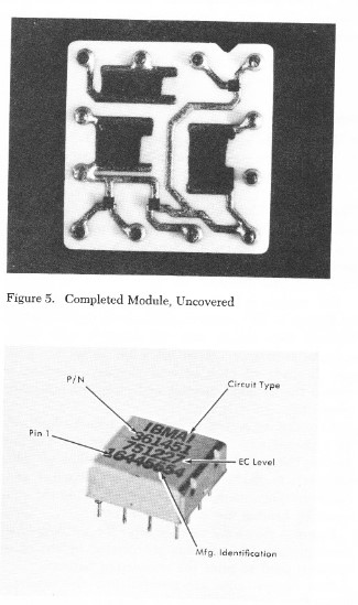
The first bookend is the ALD (Automated Logic Diagram) of the 1130 which shows all the logic gates and their interconnections. There are flipflops (FF), And-Or-Invert (AOI) gates, And gates, Not gates, edge triggered inverters, single shots, switch debouncers and dot-OR 'gates' on the diagram for the card.

The second bookend is the physical card with its part numbers on the SLT cans and other components. These indicate which are AOI, FF or other functions for which there ARE circuit diagrams. Since I know the SLT can pin numbers for inputs and outputs, plus the card pin numbers for signals, I can beep out which cans are implementing each gate from the ALD.

The card has four pins that do not show up on the ALD, but they may have some connection to an internal state that would aid in debugging or checkout at the manufacturing plant even though not used inside the 1130 itself. If I can beep out those and relate them to the circuitry, it might let me observe some internal state more easily.

However, every single connection and pin from SLT cans or other components are accessible by touching the solder pad on the rear of the card. Thus, I can narrow down to the component(s) that are failing by varying my inputs and observing the the oscilloscope. 

If I do find bad components, I have the potential to repair the card. Other cards with different overall functions may have the same SLT can that is broken. If I can remove that from a donor card and substitute it for the defective can on this card, I could get it working. Since FFs, AOI and other cans are very common elements, this should be simple to do. 

The backstop, much harder, is to make a tiny PCB the size of the SLT can, using surface mount transistors, diodes, resistors etc as a replacement that can be put on the card in place of the failed can. There would be a time lag of two to three weeks for each can to be fabricated AND it wouldn't be original components in the machine. 

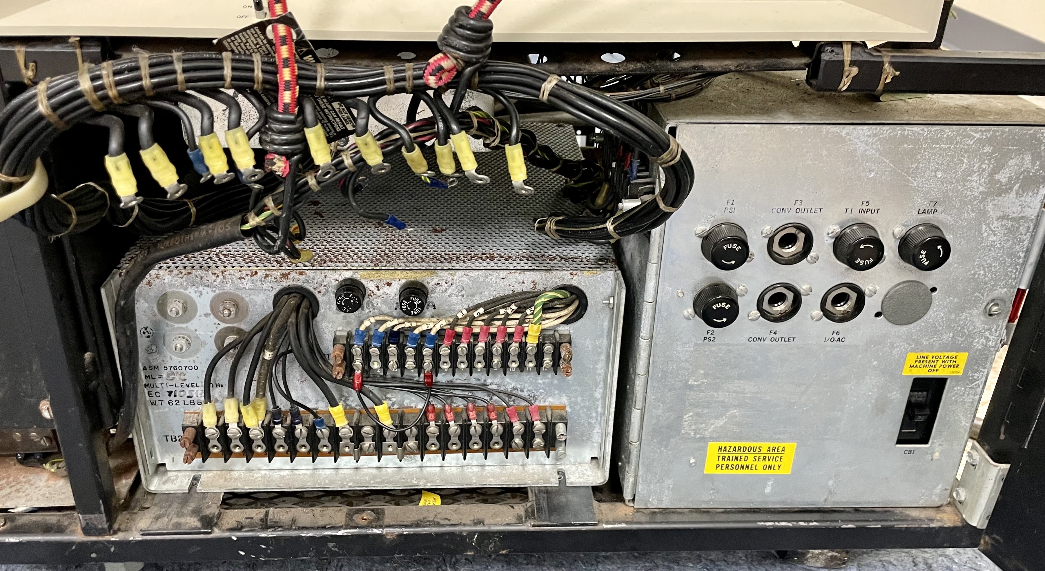
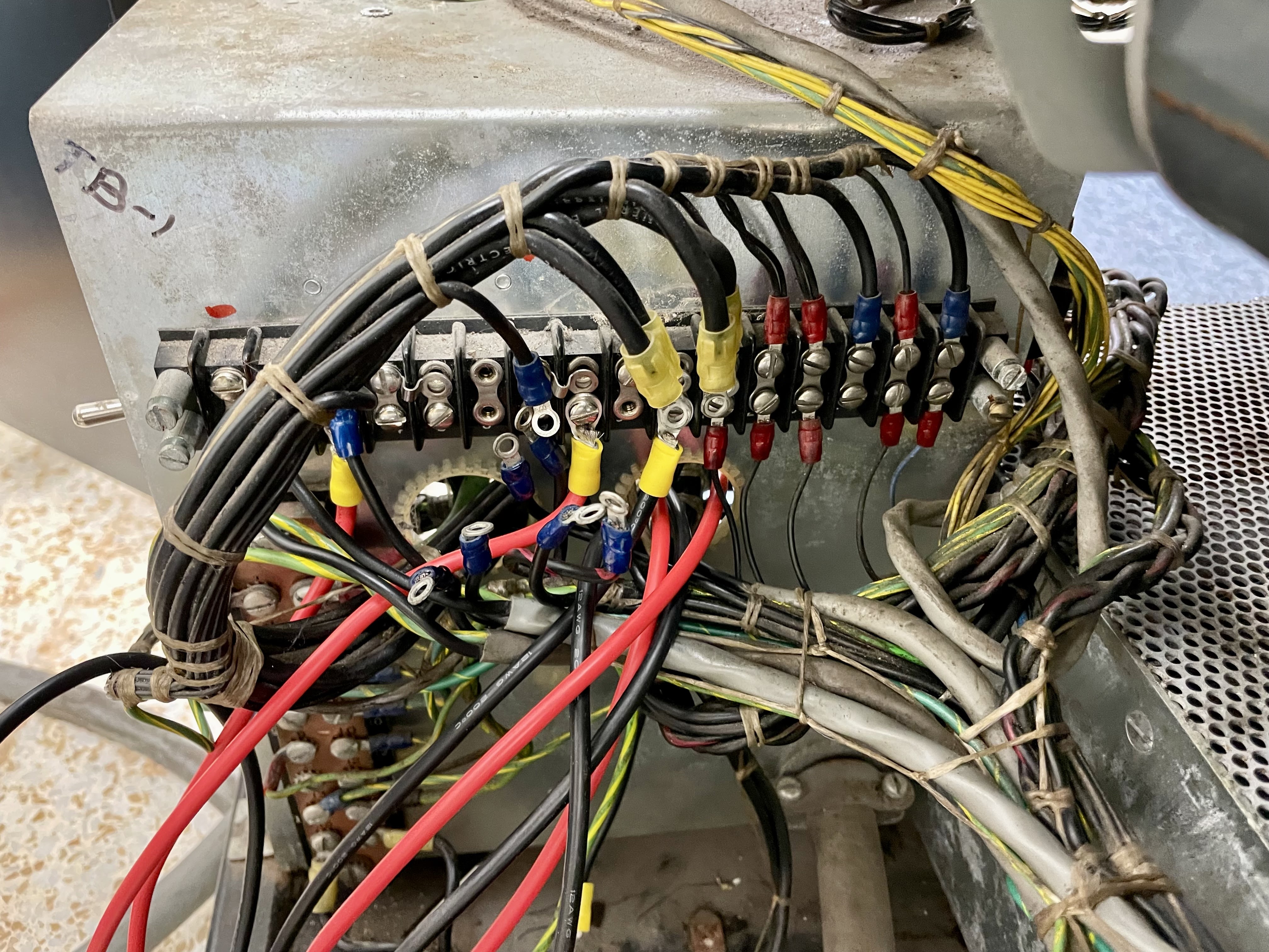
CLEANING UP THE TEST BOX AND GETTING NECESSARY CABLING

The SLT tester box I have had a modification made, introducing switches to break connections between the sockets for certain pins and the pins themselves in the card connector. The ones that were switched aren't the normal SLT power pins, so I really don't now why these mods were made.

I reversed them, so that now the sockets are all connected directly to the associated SLT connector pin. The sockets take a standard 4mm banana plug, of which I was in short supply. I have a suitable number on the way allowing me to cable up on Monday and do the testing. The banana plugs also fit into my bench power supplies, allowing a very convenient method of supplying power.

Wires with a banana plug will route various signals to a breadboard where I can implement pullup and pulldown resistors, add switches for signals I want to vary to put the card through its paces. 

Thursday, April 28, 2022

Switches/buttons in good shape, Diving into debugging of the machine state

TESTED SWITCH CONTACTS ON MACHINE

The pushbuttons and switches were all in pretty good shape, I imagine they were cleaned up by the prior restorers. Everything was good so I could move on to debugging of logic.

DEBUGGING FIRST PROBLEM

I hooked up my oscilloscope to begin chasing down the signals involved in the state machine that controls the processor starting, stopping, stepping and other basic functions. I found a signal behaving quite oddly. This signal, the Delay state flipflop, is on of a chain of three that start the machine running - Advance, Delay and Run. 

Main clock above and abnormal Delay FF signal below

As you can see from the signals, with the top yellow trace showing the main system clock at 2.25MHz, the bottom blue trace is oscillating much faster than any clock in the system. It appears to be about 12.72Mhz. I talked with the last restorer who was dealing with debugging this area of the machine. 

He mentioned that he had swapped in a card from a different 1130 system they used for spare parts. The 1130 did not work with that card either, but the symptoms were different. This suggests that at least one of these cards is bad, if not both. 

I decided to debug the card out of the machine, to simplify things considerably. So many machine functions spread across different boards and backplanes are involved in the central state machine behavior that it might require an unwieldy number of observations before I come across the problem or prove that this card is bad.

SETTING UP MY CARD DEBUGGING RIG

I have a handy appliance with SLT sockets and a breakout of each pin that is easily accessible. The SLT logic requires three power rails - +3, -3 and +6V - which I can easily generate with my bench power supplies including current limiting to avoid any damage during testing.

My SLT card debugging rig with the suspect card inserted

This card receives the oscillator at 2.25MHz and passes on clock pulses based on the run state machine inside. The double size SLT card has 38 input or output signals in addition to the power connections. The inputs are a number of machine conditions, the Prog Start and Reset pushbuttons, the oscillator input and similar state that determines whether to run, wait or single step. 

My function generator will produce the oscillator square wave that will drive the system. While I could slow down the oscillator rate that is not how the 1130 does single stepping style operations so I won't either. 

I can use pullup or pulldown resistors to set the logic levels of all the inputs and then observe the outputs to determine if there are any defective gates on the card. Conveniently I can debug both of the cards using the same setup. 

Wednesday, April 27, 2022

My plan for the next day or two will focus on validating that switches are working, not oxidized

 STATE LOGIC FOR THE 1130 DEPENDS ON SWITCHES ON CONSOLE

In some cases, both a positive and a negative signal must be generated when a switch is depressed. IBM accomplishes this with a DPDT switch whose poles produce the two opposing states. If one of them is not working correctly, as when a contact is oxidized so much it doesn't conduct, then the state machine can be very confused. 

I will therefore go through with a continuity meter, deoxidizing spray and burnishing tool to make sure that all the contacts are working properly. I will do this in four areas - the console display pedestal with its Mode rotary switch, the pushbuttons on next to the keyboard, the CE switches inside the top cover, and the console entry switches in front of the console typewriter.

Once that is done I can begin to hook up scopes and other tools to debug the state of the machine starting with the clocks and working outward. 

Discovered fault in 6V Power Supply, system powers up; beginning of logic debug

INVESTIGATING NON-ISOLATION OF DC SUPPLY 16.5 OUTPUT

The DC Supply 16.5V (nominal 12V) output should be fully isolated from any other circuit in the machine. It is produced by separate secondary windings on a power transformer, not tied to neutral, ground or any other wire. 

Bottom section (12v at 24A) is the 16.5V supply for +6V

As you can see from the diagram above, the raw DC that is hooked to the +6V Regulating Supply should be fully isolated. As such, adding one connection to the Regulating Supply cannot create a circuit and current flow with this. I did see 10V between the common output wire and the common output of the Regulator Supply, which definitely explains the flow of current and breaker triggering.

Regulating supply with 16.5 in, common wire connected only

It was time to look for sneak paths, miswired connections or component failures that might connect something in the DC Power Supply 12v at 24A section with any other wire in the 1130 such that it causes the symptoms I am experiencing.

The problem was indeed a sneak path, but not in the DC Power Supply. I had slid the +6V Regulating Supply into its mounting rails for my tests, but hadn't tightened the bolts that hold it in place. As a consequence, it sagged a bit and unbeknownst to me the heat sinks of the supply were contacting chassis ground! 

CORRECTED PROBLEM, VERIFIED ISOLATION,TESTED WITH ONLY COMMON TERMINAL 

I held it in place and tightened up the mounting bolts. These are accessible from deep inside the rear of the machine after swinging the logic gates out, just to explain why I didn't take that step initially when I was putting the supply in and out of the machine. 

The problem was gone! Time to hook up the common output lead and power up. That also worked fine, no tripping of the breaker and a solid 6V across the outputs. 

TESTING SUPPLY WITH BOTH WIRES CONNECTED, ADJUSTED 6V RAIL LEVEL

Turning on only the 6V Regulating Supply circuit breaker, but not the +3 and -3 supplies, makes it safe to energize for a brief period while I adjust the regulator potentiometer to get the +6V rail spot on its target voltage. I did set it as close to 6.00 as possible. To be extra careful, I went back and tweaked the other supply voltages to 3.00 and -3.00 as close as I could. 

BRINGING UP ALL POWER TO THE 1130

I flipped on all three circuit breakers for the logic rails, made sure the fuses were in place for all DC voltages (-3, +3, +6, +12 and +48), then switched on the processor. It came up, lights were displayed on the console panel, and I saw signs of life.

INITIAL OBSERVATIONS

The RUN lamp goes on immediately when the system is in Run mode, but putting it in single step (SS) mode kept it stopped. I suspect I may have a hot cycle steal that is forcing this to run, however other issues can cause this as well.

The console entry switches were set and indeed their values are gated into the IAR register while in Load mode. The Prog Stop button triggers interrupt level 5 just as it should. 

Of the CE controls, I found that Lamp Test worked but Storage Display did not, largely due to the machine being in a run state. There was no parity error indicated for the initial location (x0000) which suggests that at least that location of core memory is working properly. 

I smelled some smoke and found the CE Meter power box emitting wisps of smoke. I will have to check into that and figure out what is going wrong there. Fortunately this is not a mission critical function and to boot it is relatively easy to fix. 

Tuesday, April 26, 2022

+6V Power supply passes with flying colors, but something is still off here

INSTALLING POWER SUPPLIES AND WIRING THEM INTO THE SYSTEM

I closed up the DC Supply, the unit that provides the raw DC to the regulated power supplies like the one I am repairing. I slid it into the machine and began to wire up the two terminal blocks - the AC inputs side and the DC outputs, essentially.

DC Power Supply - raw DC outputs

Inserted in place, ready to wire up

TB-1 completed, TB-2 at bottom to do next

TB-2 completed, plastic safety cover on TB-1 but not yet TB-2

I then put the +6V Regulated Supply into the chassis and began wiring it up to the input from the DC Supply. I did not connect the load side - the logic circuits that are connected to the 6V rail. 

6V Regulated Supply ready to insert

TEST RESULTS WITH 6A, 12A, 18A AND 24A

With the power supply mounted in the 1130 chassis and its raw 16.5V DC input connected, I wired it to my resistor complex which lets me select 6A, 12A, 18A or 24A loading. The supply held up great, although with a bit of sag in voltage when I hit its full 24A rating. Since my expectation is that this 1130 will be closer to 15A maximum load and the average even less, I thought I was good to go. 

Resistor complex to load up the power supply

ADJUSTING +6V AT RAILS OF BACKPLANES IN 1130, BREAKER TRIPS

I removed my resistor complex, wired in the 1130 logic load. I first checked the resistance of the 6A load side and found it at 3.8 ohms, which means that the idle consumption will be teeny. With everything tidied up, I flipped on only the 6V supply, with a voltmeter on the logic backplane side to sense the delivered voltage, then powered up.

What I expected was minimal load and an opportunity to adjust the 6V rails to the middle of the target range, right on 6.00V. Instead, I heard the breaker click off immediately. This was disappointing indeed. Out came the supply and over to the bench to figure out what else had failed. 

MACHINE STILL GOOD ON BENCH AND AT HIGH LOAD - HMMMMM

With it hooked up and the 4A electronic load active, I powered it on and it was behaving properly. Perhaps it was a load based issue, thus I hauled it back over, slid it into the chassis and wired it up again with my resistor complex to give it high load.

It passed again! On a hunch, I connected only the Common (ground) side of the 6V load to the power supply and powered up. Click. Immediate breaker popping. This is quite mysterious.

The DC Supply that gives us 16.5VDC raw input should be completely isolated from the Common logic side. It is dead simple, a transformer secondary wired to a half wave rectifier and a filter capacitor. No connection from either of the output lugs to anything else in the machine nor to any kind of ground. This should be completely isolated.

However, all is not well in the world of the 1130, since the mere connection of one wire that should have zero path to the DC input causes an immediate overload and shutdown. This is going to require some investigating to figure out what has gone awry, most likely over in the DC Power Supply box. 


Monday, April 25, 2022

Testing rig for voltage regulator card being set up, believe I found and fixed the problem

CONCEPT FOR TESTING THE 6V AMPLIFIER CARD OUTSIDE THE POWER SUPPLY

Based on the schematics of the supply and the regulator card, I believe I can connect the input power supply across the K,L,M pads for negative and the positive end hooked to pad R which is the +Sense connection. Then a variable supply is set up across the +sense and -sense pads (R and Q) so that I can see how the regulator responds as the voltage is below, on and above target. 

The output of the card at B,C would be drive current that flows into the base electrodes of the bank of power transistors, returning out of the emitter through a .10 ohm resistor to the K,L,M pad side of the input power supply. I will wire up one spare 108 transistor and resistor for this purpose. For the load side I will connect a 15 ohm resistor which should draw about 600ma at the target output voltage.

I played around with circuit simulations until I felt comfortable with how this will work before I applied power and possibly damaged the card. I am ready to head over to the shop, breadboard this out and check the card.

WIRING PRACTICALITIES

I either need to find a spare SMS socket or do something more involved to connect to the various pads B, C, K, L, M, R and Q. Wiring in resistors and connections to the bench supply is easy. I did indeed have a spare SMS socket, so I was ready to go. I decided to check the Overvoltage Protection card first, just to see at what voltage it would trigger.

OV CARD HAS WEIRD HYSTERESIS BUT TRIGGERS ABOVE 6.5V

Setting my bench supply to current limit at 500ma, I began applying increasing voltages to the crowbar card circuit until it fired, latched up and hit the current limit of the supply. That seemed to be somewhere in the range of 6.5 to 6.6V, well enough above the top of the valid range for the +6V supply that it shouldn't spuriously trigger.

When it fires, it locks down regardless of reductions in the input supply. However, when I switch off the supply entirely it should immediately reset, since it is a SCR thyristor which will unlatch when current goes to zero.

However, it didn't unlatch right away. I found that for many tens of seconds after it triggered and I disconnected the power, when I reapplied even a very low voltage it would still be conducting. There are no capacitors on the card, so this is some weird internal capacitance or other phenomenon of either of the two SCRs. Not an issue, just an odd behavior.

OBSERVATION SUGGESTED MAIN DRIVER TRANSISTOR WAS BAD

Driving the regulator card with my test setup, I would see that its ability to hold the output voltage would stop at about 13.5 volts on the input, where it began to oscillate up and down with excursions well into the overvoltage trip range. 

As I checked the output, it looked to me like the driver transistor was bad - which makes sense because if it can't drive the bases of the main power transistors, they won't be able to regulate their current and establish the voltage level desired.

The other two 108 transistors which failed all exhibit a characteristic behavior on the VOM diode test setting. While a good 108 will have a voltage drop in only one direction between emitter and base, the bad transistors show voltages in both directions. I look for the open circuit to determine that a 108 transistor is still good.

REPLACED 108 TRANSISTOR, RESULTS MUCH BETTER

After I unsoldered the bad one and installed a replacement, the behavior in the test rig was much better. I moved the card over to the actual power supply, hooked up my bench supply and electronic load, then tested again. 

At 4A load, the supply held rock steady even as I advanced the input voltage from 9V all the way up to the 16.5V that comes out of the unloaded DC Power Supply in the 1130. No oscillations, no excursions, just clean behavior with nary a hiccup as I varied the load.

I am glad it was the 108, for which I have spare units, rather than the two 026, the 086 or the 123 transistors that are on the regulator card (or the two 033 transistors on the overvoltage card). It could also have been failed zener diodes, one in the regulator and one in the overvoltage, for which I don't have a written spec for the voltage level making replacement challenging. 

READYING FOR A FULL LOAD TEST IN THE MACHINE

While this looks like I have turned the corner and fixed the power supply, I can't be sure until I see how it behaves with a full load on it. I have the resistor complex that will let me set up loads of 6, 12, 18 and then 24A but the supply is going to have to be fed by something that can deliver more than 24A of input voltage. 

As I mentioned earlier, the way I intend to perform this test is to put the power supply into the 1130, but leave the load side disconnected - the logic circuits won't touch the supply until I feel it is truly solid. Instead I will wire in my resistor load complex and test it that way. If it survives the full 24A of load with steady output voltage and no overvoltage incidents, I will wire it back to the logic circuits and move forward. 

DC Power Supply for raw DC voltages

Sunday, April 24, 2022

+6V Regulated Power Supply in more depth

THIS SUPPLY REGULATES DC DOWN TO A VERY STEADY +6V

The IBM 1130 has a DC power supply that is fed input mains voltage, transforms it down, rectifies it and smooths it with large capacitors. The resulting voltages can shift up and down with changes in the building power as well as with the effects of varying loads as different circuits operate. This raw DC is fed to a set of regulating power supplies that produce regulated steady power for use with the logic.

The +6V supply is nominally fed with 12V raw DC from the DC Power Supply, although in our case it is actually up at 16.5V. The negative side of the input is fed into this regulator and the positive side of the raw DC is tied to the positive output terminal. Thus the supply acts by moving the negative or common output terminal to be six volts below the positive output. 

The output transistors will conduct enough current from the negative side of the input to bring the common output to zero volts. The regulator circuit is on another SMS card and will drive the output transistors based on what is needed to keep the difference across the output at the target set.

It does this starting with a differential transistor pair that uses a zener diode as a reference voltage on one side and a potentiometer adjusted fraction of the output voltage on the other side. The power transistors are then driven by other circuitry so that it keeps the differential pair essentially balanced. 

You can think of this as a kind of servo or feedback mechanism, with the regulator card producing an error signal that is amplified to a strong drive signal for the output transistors. IBM's official name for this SMS card is "6V Amplifier".

Redrawn schematic used for circuit simulation

FOLDING AND STACKING A CHAIN OF SIX OUTPUT TRANSISTORS

The supply puts each output transistor on its own heat sink, along with an emitter resistor that causes the transistors to balance the load among the various transistors. The emitter and base connections are daisy chained with appropriate thickness of wire, producing a long train of heat sinks initially. 

Six heat sinks each handling 4A of output current

These are then placed side by side and electrically connected by a heavy aluminum bar spanning the heat sinks. If all six were linearly placed the supply would take up too much real estate, so the design will place three across, then fold the chain to run back in the other direction for the next three. These are therefore stacked, two levels of heat sinks, to fix all six in a reasonable volume. 

First three in place, layer one complete

Full stack assembled
+
CHECKING OUT DC POWER SUPPLY

I removed the DC Power Supply to be sure there was nothing wrong there that led to the 16.5V output. This box feeds raw power for +3, -3, +6, +48 and +12 thus is large and extremely heavy. I wanted to be sure there wasn't a problem with the windings involved in 230V operation, or with the rectifier diodes. 
DC Supply removed, all the wiring in place.


The diodes are good and even when I rewired and hooked it up to 115V, the output was the same stepdown ratio. Thus, this is the level the supply is going to be dealing with, so the focus remains solely on the regulator card.

Overvoltage protection is essential with rare vintage computers

OVERVOLTAGE PROTECTION - CROWBAR CIRCUIT

Because excess voltage can break down junctions of transistors and diodes, said parts being in extremely limited supply, it is essential that power circuits in vintage systems like the IBM 1130 have a means of detecting any deviation upwards in voltage and cutting it off very rapidly.

The method used in these systems is to short across the input to a power supply when the output voltage exceeds some threshold, this short circuit causing the circuit breaker to trip very rapidly. This is termed a crowbar circuit, alluding to the method used with electrified railways to quickly kill power by tossing a metal bar across the power rails to force fuses to blow. 

IBM's power supplies are built to use an SMS card that is set with a zener diode at some threshold above the nominal supply voltage. For example, it might be set at 7.2V to give a bit of margin for power supply swings while crisply acting on any larger excursion. The zener diode sets a reference voltage on one of a pair of transistors, the other side of the differential pair is sensing the supply voltage. 

When the supply side exceeds the reference side, the differential pair swings over to the side that is connected to a SCR (Silicon Controlled Rectifier). The SCR will latch on and remain conducting until all power is removed from the system. 

Because the power supply being protected is high capacity and protected by a 30A circuit breaker, the SCR must be able to absorb more than that for the time it takes for the quick trip breaker to flip off. The IBM SMS card actually uses a pair of SCRs - a smaller one that will conduct immediately based on the relatively sensitive differential transistor pair, which in turn will feed enough current to trigger a major 80A rated SCR. 

THE FAILURE IN THE 6V REGULATED SUPPLY CAUSED HIGH VOLTAGE SWINGS

What I observed in the power supply on the bench was that with the relatively high input at 16.5V, the supply would be unstable, the output voltage surging up over 7.5 volts regularly. This in turn would cause the overvoltage card to latch the SCRs on in an attempt to trip the break. 

Since my measly 5A bench supply couldn't deliver the high current needed to trip the breaker, we just went into current limiting mode and the input voltage sagged. When hooked to the real IBM 1130 supply of 16.5V, with its ability to feed serious current, the breaker tripped almost instantly. 

TRIPPING BREAKERS RATHER THAN DESTROYING ELECTRONIC COMPONENTS

Tripping a breaker in milliseconds, while lowering the output voltage to nearly zero in much less time than that, means that sensitive junctions don't have time for heat effects to damage their junctions. This keeps a power supply malfunction from destroying hundreds of SLT cards. 

Saturday, April 23, 2022

108 Transistors arrived, power supply back together but still not working correctly

RECEIVED MY FIRST BATCH OF 108 TRANSISTORS AND TESTED TWO UNDER 4A LOAD

I serially installed two of the new transistors in one of the heat sinks and verified that the unit would support the full 4A load with steady output voltage. With all the main transistors now working properly it was time to put things together and finish the testing.

REASSEMBLED POWER SUPPLY AND FAILED WITH TEST AT FULL 24A RATING

My bench supply can't deliver 25A to test this out so I had to take advantage of the 1130 which can feed that much. I hooked the 6V power supply into the 1130, but instead of connecting its output to the logic circuits I hooked it to my resistor complex at the initial load level of 6A.

The breaker immediately popped! I pulled the unit and put it back on my bench power supply, where it worked properly again. At this point I started to look more carefully at the supply of the raw voltage that is fed to the unit in question. 

The 1130 power system is divided into two halves. One part has transformers, rectifiers and capacitors, producing raw unregulated voltages at different levels to be fed to the other part, the regulator supply. The unit I am repairing is the regulator supply. The first part shows its output as 12V on the ALDs and other documentation, but measures 16.5 volts in real life. In fact, all the raw voltages are a bit high, the 48V raw runs at 52.5, the raw 12V is at 13.9, and the raw 3V supplies sit at around 7. 

I increased the voltage of my bench supply from the 9V I had been using up to 16.5V, where I immediately saw the power supply try to trip the breaker. It couldn't because my bench supply is current limited at 5A, therefore the supplied voltage sagged instead. 

CHECKED WHAT IS HAPPENING AT HIGHER INPUT VOLTAGES

My testing focused solely on whether the output voltage remained constant as I varied the load, up to the realistic limits of my bench setup which is around 4.7A. I hadn't looked at higher raw voltages on the input, but this appears to be the issue.

With experimentation I discovered the supply is happy up to about 12.5V of raw input, but above that the output voltage starts varying upwards, quickly triggering the overvoltage protection which would trip the breaker if we weren't current limited. With over 16V coming from the raw supply the breaker will trip as it did repeatedly. 

I grabbed the small DC-DC supply that had been wired into the 1130 by a past restorer. This unit is claimed to support up to 20A which should allow me to test at loads up to 18A with my resistor complex. I wired it into the line between my bench supply set to 16.5 and the regulator supply I am testing, with the DC-DC board set to 11.5 volts output. 

At 4.7A load, this held steady but when I tried increasing my electronic load to 6.7A, I saw everything sag. Measuring the voltage at the input of the regulator supply showed it dropping well below the 11.5V that it should be outputting. It appears to be current limited quite a bit below the faceplate capacity of 20A. 

NEXT UP - TROUBLESHOOT THE VOLTAGE REGULATOR BOARD

The likely culprit in all this is the voltage regulator board, an SMS card with five transistors and a medley of other parts, which should be modulating the drive of the six main transistors to delivery steady power at the target voltage. 

Friday, April 22, 2022

Found and corrected miswiring of 1130 metering power supply, adding Console Loading Automaton

IBM 1130 CUSTOMER USAGE METER POWER SUPPLY LEFT AT 115VAC SETTING

The IBM 1130 with its three possible 60Hz supply voltages of 115, 208 or 230 has a number of transformers whose windings must be selected to match the voltage, so that the output is the intended level, e.g. 48V regardless of the choice of mains supply. 

Enough that it requires quite a bit of diligence to be sure that you have set all of them properly when changing a machine between different voltage levels, as I did switching my own 1130 from 208 to 230 and as this machine must do to change from 115 to 230.

I was suspicious of the usage meter supply because the case has an 'anti tampering' plastic insert which is almost always broken off when a modern day owner has opened the case, but it was intact on this system. I doubted that the past restorers were in possession of a tool to open this piece or even aware of the purpose of that plastic bit.

IBM rented computers rather than sold them until they agreed to a 1950s era consent decree with the US Department of Justice that ended up shifting the business to almost exclusively outright sale or long term lease. In support of rental, IBM configured their systems with usage meters that would count the hours and tenths of hours that a machine was running. This allowed customers to choose lower priced 'one shift per day' rental rates or around-the-clock but higher rates. 

When IBM maintained a system, a second CE usage meter was switched on so that the hours spent doing repair were not billed to the customer. This is why you see to meters with a keyswitch in between them; the CE would switch over when they took the mainframe for service and switch it back when returning it to the customer. 

Since the hours recorded were important to the revenue, IBM sealed the circuitry that switched between CE and customer mode, as well as powered the meters. The box with the power supply and logic for the usage meters had a plastic security tab inserted that would break off if an unauthorized (or not criminally clever) person opened the box. 

When I opened the box I found the wiring still set for 115VAC. That means that the hour meters were receiving double their designed voltage and the control circuitry was as well. Fortunately, there are no transistors or other particularly voltage sensitive parts inside, just relays and resistors and diodes, thus I expect this has survived the overvoltage. It is now set to 230VAC for future operation. Whether the hour meters have suffered any damage will have to wait until I am running the system to determine. 

CONSOLE LOADING AUTOMATON TO BE ADDED TO THIS SYSTEM

To help out a UK museum that has a running IBM 1130, I developed a small tool based around an Arduino and a few relay boards that would let a PC based text file drive this to load core memory with whatever contents were desired. This was much faster than manually flipping the console entry switches on the 1130 and pushing the buttons to load each word, thus making it practical to load in decent sized programs and data. 

I don't need this on my own 1130 because my FPGA based extender box makes use of cycle stealing (DMA) to load and dump memory at even faster speeds, but for the system I am restoring, I will add this capability. Essentially this flips the entry switches and pushes the Program Start button to load the data into a memory location. It also flips the entry switches and pushes the Load IAR button to set the next address for a block of data to be loaded. 

The Arduino communicates over the USB serial link to a remote system which can issue the commands I defined to set the IAR and to load contents into memory. 

The protocol is extremely simple. You transmit lines with four hexadecimal characters to have that word loaded into the current IAR. The 1130 system will automatically advance the IAR after loading a word, thus the next data goes into the next sequential address. Prefixing a word with @ will take those hex digits as an address and load the IAR with them.  Without a prefix, this is a data value to load.

A prefix of # will take control over the 1130 for loading (activation), however if already active then it will return control (deactivation). This allows the link to remain active between the terminal/PC and the 1130 system, allowing normal console operations until it is activated. 

Going to replace the stepdown transformers in the IBM 1130 being restored

INADEQUATE TRANSFORMER CAPACITY RAISES SAFETY ISSUES

Portions of the IBM 1130 system require 115V supply thus when a machine is configured to attach to 208V or 230V mains, stepdown transformers were used in the machine to deliver the lower voltage. Specifically, two transformers T2 and T3 are configured in machines that attach to higher voltages.

Transformer T3 is used solely to power some convenience outlets, the normal US household duplex outlets, which are inside the covers of the IBM 1130 processor and inside the 1442 Card Reader/Punch. These are generally used to power oscilloscopes and other test gear, but have been used for vacuum cleaners and floor washing machinery in data centers. 

The transformer has its primary inputs protected by fuses F3 and F4, thus limiting the current that can be drawn through all the attached convenience outlets to a maximum of 6.5A at 115V. The transformers that are installed in the machine right now are rated at 300VA, thus they cannot support the roughly 750VA that the outlets could pull. The result in that situation is that the transformer overheats, perhaps is damaged but in the worst case could burn. 

Temporarily, I am protecting against that risk by lowering the fuse sizes in F3 and F4 to keep the load within T3's 300VA capability. Longer term, I will purchase a new stepdown transformer good for at least 750VA and place that in the 1130 along with the original fuse sizes. 

Transformer T2 is used to provide 115V to a number of destinations in the machine, per the design, plus one additional load that is unique to this machine. As designed by IBM, this transformer provides 115VAC for the cooling fans in the machine. It also provides 115VAC for peripherals such as the internal disk drive, the console printer and in other system devices such as paper tape peripherals or plotter. 

Since our machine has had most of its cooling fans in the 1130 replaced with 230V motors, they no longer are attached to T2. On the other hand, the lighting power supply that is used by all the incandescent bulbs behind the main display panel is a part that comes in two types. One type is 115VAC only, the other type is only 208 or 230V. Since this machine was originally configured for 115VAC, I had to provide the power to this supply from T2.

The primaries for T2 are not protected by fuses. Instead there are fuses to limit some but not all of the draw on it. Fuse F7 limits the 115V load for the incandescent light power supply to 1A. Fuse F6 limits the load for the console printer motor, disk drive motor, and disk drive cooling fan to 3.25A. These sum to almost 500VA which exceeds the capability of T2 even without it driving the seven cooling fans in the processor box. Without blowing fuses this could produce overheating and perhaps burning of transformer T2.

I will replace this transformer with one having sufficient capacity to power all the gear and the original 115V cooling fans, even though I won't convert back to those fans at this time. 

Thursday, April 21, 2022

Finishing wiring of the console panel lighting power, tested and closed up fpga extender box for other 1130

IMPLEMENTING FUSE FOR THE LIGHTING PANEL POWER SUPPLY

I disconnected the feed to fuse F7 which was fed from the 230V line after the power contactor. The various fuses have wires with terminal rings that daisy chain the power between the fuses that share a source. By moving one wire that runs to F7, taking it off F2 where it was tapping the 230V supply and moving it to F6 which is tapping the T2 115V supply, I 'converted' the fuse to a 115V feed which can go directly to the terminal block to connect to the lighting power supply.

The only change that needed to be made was to swing the common side wire from where it was placed on the terminal for the 230V common and move it one down to a common for the 115V out of T2. I now have a properly fused supply that will be getting 115V when the machine is powered up.

TESTING SUPPLY AND OUTPUT VOLTAGE OFFLINE

I wired up a temporary plug to 115V with a 1A fuse and wired it to the power supply, having disconnected the wires from the 1130 power distribution box. This allowed me to fire it up and verify the correct operation and output voltage before I hooked it to the system.

Indeed, the supply worked without blowing the fuse and produced a bit over 7.25VAC on its output. All appears good so I proceeded to wire this into the machine, put in fuse F7 and power up the 1130.

VERIFYING LIGHTS WORK ON DISPLAY BOARD

Once this was up and running I hooked up a small bench supply to deliver 3V through a 6.2Kohm series resistor to various lamp input pins of the control board. I of course verified that the black terminal of the bench supply did not carry a voltage relative to the lighting board common terminal, since that is the return side of the 3V I will inject. 

I found about 15VAC across the grounds, clearly something picked up from the neutral side of the AC supply to which the bench supply was connected. I quickly solved that problem by putting in the fuses to active T3 and the convenience outlet. With the bench supply plugged into that outlet, I have isolation of ground and could wire the 'ground' or return terminal of the bench supply to the shared ground in the lighting panel circuit.

When I touched the 3V fed through the resistor to various signal pins, the lamps lit exactly as expected. I feel confident that most if not all will display when I get the +6V supply repaired and back into the machine. 

FINISHED CONTINUITY TESTING OF CABLE CONNECTORS TO THE FPGA BOARD

My FPGA based extender box connects to my IBM 1130 using the Storage Access Channel cables plus an augmented set of functions I added on a separate cable. I finished up the testing of the wiring and closed up the box. Next steps are to move it over next to my 1130, and cable it up. 

Wednesday, April 20, 2022

Finished AC rewiring, had an issue with the console light power supply that needed addressing

COMPLETED TB-1 WIRING WITH MODIFICATION

I implemented the split where the fans are grouped on the 230V line, jumpered over to the section of the terminal block for 230V, while the 115V output of T2 is reserved for the 1053 typewriter motor. Or so I thought - more later. 

COMPLETED TB-2 WIRING

Similarly, I finished putting the TB-2 wiring inside the power distribution box back to its original layout. This involved tracing every wire with the continuity checker to be sure that they were all in their correct places. 

DISCOVERED THAT THE DISPLAY PANEL LIGHTING POWER SUPPLY IS 115VAC

Having restored the wiring for the 7.25VAC power supply to the circuit fed by fuse F7 and having a suitable low current fuse in place, I turned on the machine to verify the lighting voltage was present. Nothing. In fact, the fuse blew!

I looked at the diagrams to see if this was wired improperly or was set up for 230V. That is when I noticed that IBM didn't provide the ability to switch the supply between 115V and the higher voltages. Instead, they ship either a 115V supply or a 208/230V supply. Reading the part number quickly confirmed that it was the low voltage version. 

IT APPEARS THIS MACHINE WAS ORIGINALLY CONFIGURED AS A 115V SYSTEM

This explains a lot. No wonder I didn't find the Ferro Resonant transformers used by IBM, instead finding some low capacity alternatives in place. When a machine is ordered for 115V, IBM does not include the transformers as there would be no need to step down voltage. 

A prior restorer converted this to 230V, adding the transformers and swapping all the fans to 230V versions. That left the AC wiring inconsistent with the wiring diagrams and usual IBM practice.

MODIFYING THE TB-2 AREA TO SUPPORT THE LIGHTING SUPPLY

Since transformer T2, normally providing power to fans as well as the 1053, is underutilized right now, I found a scheme that would let me move the lighting power supply over to the 115VAC fed by T2. This involved adding a metal jumper and moving a couple of wires around on TB-2. 

Tuesday, April 19, 2022

Rewiring of transformers completed, rewiring of all AC connections underway, load tester prepared, blower voltage verified

ROMEX REMOVED AND IBM STYLE WIRING INSTALLED FOR THE TRANSFORMERS

As I mentioned previously, the use of ROMEX style wiring is inconsistent with the wiring methods used in IBM mainframes in the 1950s, 1960s and 1970s. I decided to rewire with 12 gauge stranded single wires, wrapping them together with lacing much as IBM did during manufacturing.

Rewiring the transformers and lacing the wiring bundle

REWIRING BOTH TERMINAL BLOCKS THAT HANDLE AC POWER CONNECTIONS

I have disconnected all the wires and am proceeding slowly and carefully reconnecting these in accordance with the original design. This will return the machine to the condition it would have had upon installation in the customer's location.

TB-1 on rear of power distribution box

TB-2 inside power distribution box

LOAD TESTER FINISHED AND READY WHEN THE POWER SUPPLY IS REPAIRED

I completed all the cabling to produce my resistor complex to load down the 6V power supply for its final testing. This design has four segments, each draws 6A and they can be connected in parallel to draw 6, 12, 18 or 24A. 

Each black lead adds a 6A load across the two long wires

REMOVED AND VERIFIED VOLTAGE OF BLOWERS IN THE MACHINE

The fan assembly underneath the midpack voltage regulators was easily removable, which allowed me to see the dataplate on the fan motor and verify exactly what voltage these operate at. It is 230VAC. 

IBM fan was replaced with a 230V version

Removing fan assembly from under midpack regulators

IBM thoughtfully designed the 1130 so that it could be connected to three different mains voltages - 208, 230 and 115. Most of the transformers inside power supplies had multiple taps, selected by moving wires and connecting jumpers to configure for the appropriate voltage. 

There were a few items that were 115VAC only, due to limitations of the components themselves or to simplify IBM's supply chain. The fans that cooled the system were 115VAC, thus a stepdown transformer was included for any system that hooked to 208 or 230 mains supply. The motor in the selectric typewriter based 1053 Console Printer ran on 115VAC. 

Finally, to standardize the tools that IBM deployed throughout their organization, all tools were 115V. To support use of these tools, IBM had convenience outlets inside most of their machines which let the field engineers plug in their tools regardless of the voltage levels used by the rest of the machine. A stepdown transformer produced the 115VAC for convenience outlets.

This machine had the original IBM fans removed and new blowers installed that ran on 230V, thus obviating the need for stepdown transformer T2 to produce the 115V to run cooling. However, the transformer is still used to deliver 115VAC to the 1053 printer and it supplied over the power cable to the fans on the IBM 1442 Card Reader/Punch. Fairly wasteful but this is the only way to drive the typewriter motor. 

ISSUE SPOTTED WITH THE CONVENIENCE OUTLET TRANSFORMER T3

The second stepdown transformer T3 is provided to deliver 115VAC to the standard US style duplex outlet. IBM shipped only 115V tools to its FEs, who plugged them into these convenience outlets. Thus, any machine hooked to 208 or 230V mains had to step down the voltage to support the outlet. While a single transformer could have supported the fans, the typewriter motor and the convenience outlet IBM chose to isolate these so that if the convenience outlet blew a fuse it didn't stop the fans from operating. 

While I was wiring these up and fastening them down so they didn't slide around inside the computer, I noticed that the data plate identifies the capacity of this transformer as 300VA. For a 115V convenience outlet, this allows only 2.6A of current, not the full 15A one would expect from a standard duplex outlet. IBM configured the fuses for the convenience outlet transformer at 6.25A to the primary of T3, which supports 12 1/2 A or more at the outlet. I am going to drop the fuse used for this circuit to 1 4/10 A as that will match as closely as possible to the capability of this substitute transformer. 

PLANNED TO REWIRE SLIGHTLY TO HANDLE THE 230V FANS

Because of the use of 230V fans, they must be hooked to different locations than originally designed. The factory shipped systems had six positions on the terminal block assigned to the 115V output of transformer T2. That was hooked to the fans in the logic gates, the fan circuits to peripherals such as the 1442, and to the SMS based power that feeds, among other devices, the motor of the console printer. Each set of three positions is jumpered together and hooked to one side of the T2 transformer output. 

With metal plate jumpers, we have the transformer hooked to one terminal and the other five available for fans and other power destinations. The 230V supply comes out of the power distribution box and hooks to two pairs of terminals. Each pair (7&8 or 9&10) is jumpered together. The input power to transformer T2 is fed from these terminals. They also provide power to most of the fuses on the distribution box and provide 230 to circuits for peripherals such as the 2501. 

The four terminals on each pair for 230V can't easily sustain another three connections each for the fans. Since the fans are not going to be connected to the T2 output any more, I reassigned some of the terminals on the strip. Now, terminal locations 1 and 2 will be jumpered by wire over to the 230V on 7&8, while terminal locations 5 and 6 will be wire jumpered to terminals 9&10. I removed the metal plates bonding these to terminal locations 3 and 4, which remain assigned to the 115V output of T2. 

Terminals 3 and 4 carry the 115V to the SMS connector for the 1053 Console Printer motor, as well as to the fan power pin for the 1442 Card Reader/Punch. 

Jumpers to bring 230V over to the fan screws on terminal block

While this sounds simple to execute, the challenge is that IBM's cables are carefully cut to length and laced together so that each wire end naturally reaches its destination terminal on the block. Because I have moved some things around slightly the wires don't fit so naturally to their new destinations. 


Monday, April 18, 2022

Short work session, finalized configuration check, unwired AC terminal block and put together resistors for load testing

SHORT SESSION TODAY

Today is the due date for filing individual income taxes in the US. I had prepared the taxes a few days ahead - it was pretty complex with the move between states, sale of the house and other events - and attempted to electronically file Friday night.

The return was rejected by the IRS, claiming that another return has already been filed under my taxpayer ID number. This is probably some kind of fraud where someone filed a return asking for a refund, claiming very little income. I have to deal with this, however.

I put a freeze on my credit agency files to protect against someone using the same identity information to attempt to sign up for credit under my name. There was no recourse other than to file by mail, including an affidavit that identity fraud was involved in the 'prior filing' they mentioned. This involved printing scores of pages of forms, signing and putting it all in a large envelope. 

The state return to California also had to be filed by mail. This was even more pages printed, both the CA forms and a copy of my federal filing, in its own large envelope. For reasons too arcane to cover here, California won't accept a check from me thus I also had to send an electronic payment to match the amount due. 

This morning we had to visit the post office, ensure the postage was correct and mail it off on the due date. From there, our overly shaggy dog had an appointment for grooming that extended into the mid afternoon. 

CHECKING THE PRESUMED CONFIGURATION BY LOOKING AT SMS PADDLE BOARD

The 1130 has a small metal plate that holds SMS sockets where various peripherals are connected via SMS paddle boards. The first two positions on the plate are assigned to the 1053 console printer, the remainder are used for the 1134 paper tape reader, the 1055 paper tape punch and the 1627 plotter. There were no sockets or wires except for the first two positions, which proves that this machine did not have 1134, 1055 or 1627 attached.

CHECKING PRESUMED CONFIGURATION BY LOOKING FOR ASSOCIATED SLT CARDS

I swung out gate A and opened compartment A1 to check for the cards that are associated with the 1231 Optical Mark Reader. On my own machine, these card positions are empty but on the 1130 I am restoring the cards are all in place for the 1231 controller logic. 

With all these checks, I can now confirm that this is an IBM 1130 model 2B, 8K core at 3.6us memory cycle time, featuring the 1053 printer and keyboard, the 1442 reader/punch and a 1231 optical mark reader. It had no other peripherals attached or configured into the system. 

BUILDING RESISTOR COMPLEX TO LOAD THE POWER SUPPLY

I soldered together the 1 ohm 10W ceramic resistors I bought to form 1 ohm blocks that can handle 40W of load - two resistors in series, plus another two in series, both pairs hooked in parallel. These four 1 ohm blocks are mounted on terminal blocks so that I can wire them up with heavy gauge wire in a few different ways. 

If I hook just one set of resistors up, it draws 6A from the supply. Two sets in parallel bring the load up to 12A, three sets get me to 18A and all four together will draw the full 24A that the supply is designed to deliver.  

resistor load complex to draw 24A

I am almost done, I just need to cut and install the lengths of wire that allow me to select how many resistor sets are in circuit and that connect this load complex to the power supply.

UNWIRED THE AC TERMINAL BLOCK IN THE POWER DISTRIBUTION BOX

The terminal block TB-2 inside the power distribution box connects various fuses and power lines to destinations throughout the machine. Since I found several connections to be incorrect, I decided the best course was to detach all the wires, beep out the other end of each and then place them back on the proper location on the terminal block. 

I had previously verified that positions 1 and 2 were properly wired, but encountered errors when I hit 3-4 and 5-6. I left the first two connected. These hook the fuses F1 and F2 to the raw DC power supply inputs. One of the inputs produces the +6, +3 and -3 supply raw power (the 6V raw power is close to 8V coming from this supply but is regulated down to +6V in the power supply I am repairing). The other input produces the +12 and +48V power which is used for functions such as driving relay coils. 

All the other connections were removed from the terminal block strip and the screws placed in a plastic box. The next time I go to the shop I will find the proper wires by beeping and screw them down where they belong. When this is done, I still have to fix up the TB-1 terminal block that sits outside this box on the rear. 

REPLACING ROMEX CABLE WITH MORE TYPICAL STRANDED WIRE

The two transformers that were replaced in this machine by a previous owner are both stepdown from the 230V supplied from the wall to 115VAC for various purposes. One of them supplies the convenience outlets on the 1130 and attached peripherals. The other supplies 115V for fans and other elements that require this voltage. 

These substitutes were wired into the TB-1 and TB-2 terminal blocks using ROMEX cable, stiff solid conductor wires in a plastic sheath. This is the wire that is used inside walls in homes to distribute power to outlets and switches. 

out of place Romex cable

Inside the IBM mainframes, however, they didn't use solid conductor wire for power, the always used stranded wire covered in plastic. The 1130 has all of these individual stranded conductor wires laced into bunches that are routed like cables throughout the machine.

I am removing the romex and installing some stranded conductor wires that are similar to the ones used by IBM. This will make the machine look more consistent with the way it was originally constructed.