Monday, November 7, 2016

Developed new approach to handling the clock and data signals from the drive

ALTO DISK TOOL

I spent a couple of days examining different ways to handle the incoming ReadClock and ReadData signals, to deal with the imperfect timing of the real disk drive. That is time between clock pulses is not a constant 600 ns. Further, if the signal changes just at the clock edge, we might have an unstable state for a short time which could confuse my state machines.

Dealing with asynchronous incoming signals is challenging, once you go down the rat holes imagining all the conditions you might face with your logic. The key is to develop logic that results in the correct state or answer in spite of the various conditions you imagine.

My clock state recognition machine is now driven by finding three of a given value in a row to swing the state of the clock to one of the binary states. That is, each on or off signal value moves us 'rightward' or 'leftward' between four conditions - clock value 0, intermediate 1, intermediate 2, and clock value 1.

As long as a condition has three states the same sequentially, we reach the side that reflects that incoming signal. One or two conflicting states in a sea of the contrary states will dither slightly off the end points but never reach the alternate end point.

Our clock signals are on for a minimum of 100 ns coming from the Diablo, which is approximately five cycles of the FPGA. We should read the on state of the clock during that intervale. The off condition is a bit less than 500 ns or 25 cycles of the fpga.

Since this state machine has two indeterminate, intermediate states between the valid off and on states, I have to be mindful that any other FSM which depends on the clock state be written with this reality in mind.

The next FSM is the one that recognizes whether we got a ReadData value of 1 during a particular bit cell (interval between clock pulses). It can use a similar strategy where it takes three or more of the same value to drive the FSM to the on or off endpoints.

However, what I truly care about is whether the machine ever reached the on endpoint during the bitcell time, regardless of its current value. It can swing to on for a short time, then swing all the way to off, but we have to remember that we saw a '1' in order to insert the appropriate bit value into the deserializer.

The third piece of this machinery that is critical is the FSM which decides when to recognize that we had a 0 or 1 bit cell. This must reliably detect when the bit cell has ended and also must keep an eye on the ReadData machine to see if we ever reached the on state during the cell.

This third machine was the most critical of all. After many false starts and alternate approaches, I settled on one that I believed would give the most reliable results. It was all done and time to start testing, although the extensive redesign made it unlikely it would all work properly first time around.

The fourth machine must detect the first 1 bit that turns on sync when we begin to read a record, going through the preamble of many zeros until the 1 bit flags the start of data words. I will retain the existing machine for now, as it appears sound to me.

When doing major changes, one has to wait to see how the tool appears to be misbehaving and then develop all the instrumentation needed to attack the problem. I was iterating to set up logic analyzer signals and test the new logic through the evening. 

Saturday, November 5, 2016

Possible situation causing misreads

ALTO DISK TOOL

I spent the day poking at various locations, observing the signals and trying to find a cause for intermittent checksum failures at these sectors. Nothing jumped out at me but I will keep looking for a clue that is reproducible and can be clearly tracked to a cause.

My working hypothesis is shifting of the clock timing. There is a specific point where the clock pulses don't arrive 600 ns apart, right before two data bits that sometime clock in as 1100 and sometimes as 0110 meaning I am skipping a clock cell ahead sometimes. The later pattern, 0110, when it sees an extra 0 value that doesn't exist, is when the checksum error occurs.

Sometimes this is captured as  01101100 and sometimes 01100110 
Clock bits where this happens are irregularly spaced

Therefore my logic to recognize clock pulses, set up the data bit values, and push them into the deserializer has some weakness that is triggered by the slightly deformed timing of clock pulses. I will have to stare at the state machine, change the data being emitted to the logic analyzer, and test some more to spot where it goes awry.

Looking at the two sides of the differential amplifier decoding the head signals,we see the following:

one side of differential amplifer

other side of differential amplifer
The signals from the differential amplifer look well formed and about the same, except for a bit of bias (notice the one bit at left is rising peak to peak in the bottom scan, but is more flat peak to peak in the top scan). I can't do anything with this observation (yet) but am saving it just in case it becomes relevant later.

If somehow the decision to count extra bit cells is due to a weak process in my fpga logic, then I could improve reading quality by redesigning this part of the hardware. I will look into a different way to handle the incoming ReadClock and ReadData pulses that might avoid this problem.

Thursday, November 3, 2016

Inconclusive investigation of one sector that receives checksum errors

ALTO DISK TOOL

Today I am going to dig deeper into sectors that had checksum errors while being read, to see if I can spot anything in the signal which preserves the real information even though it foils correct reading. Potentially, there are conditions which I could recognize and improve the successful reading rate, but it all depends on why these sectors fail.

I set up the logic analyzer to trigger the oscilloscope at the start of reading a sector, employing various delays to look at different portions of the incoming signal. The scope can look at the output of the differential amplifer, which should show the actual magnetic flux reversals on the disk surface. It can also show the separated data bits.

I picked on of the sectors and triggered the scope to capture what was occurring, both as ReadData bits emitted from the separator and as raw transitions from the disk surface. I found a spot in the Label record where I could see a bit that appeared or didn't over multiple reads.

I moved the scope to focus more on this time and verified that the bit appears or is hidden on different passes. It is consistently that one bit in this area that pops up or does not.

Region when bit is not detected
Same region, extra 1 bit shows up

I then looked at the raw transitions relating to this and began to study them for signs of some anomaly. Note that it is the Diablo hardware which is responsible for this bit appearing or hiding, not my logic. The signals above are sampled from the incoming ReadData line.

Anomalous region where the random bit appears


A region with all zero data bits correponds to a flux transition every 600 ns, as show below. The spacing is nice and regular as are the voltage swings.

Waveform during string of 0 data bits
Next we look at a region with some 1 bits mixed in, to see what the waveforms look like. I have included a diagram of what we should see as input and the effect it has on recovered data bits.

Some 1 bits, adding transition between the 600 ns clock swings
What mixed waveforsm should look like and bit recovery

Repeating our anomalous region to compare to the waveforms, we interpret it based on the midpoint of each transition. Using the centerline as time 0, the bit cell with a data value of 0 ends with the transition at 250ns. The cell with a 1 data value has the extra transition occuring at 550 ns and is completed at 850ns.

Repeat of suspect signal

We see another transition at 1150 ns, which is the timing for another 1 bit. The end of that bit cell is at 1500 ns, close to when it should occur. The next transition is a 2150 ns, consistent with a bit cell containing a 0 data bit. .

I have to conclude that this is not an anomaly at all, but a pair of 1 bits. I was catching the wrong part of the signal on the scope. I had to retest and shift round the scope to find the location with the random bit value. Somewhere to the right of 561.9 us where this picture took place. 

The captured spot is a clean 1 bit, so I went back to watching the output of ReadData to see if I can spot it failing to output the 1 value.

I did see that this sector will sporadically get a Header record checksum failure, often enough to watch for differences in the delivered bits on ReadData. This is easy because one of the two words is 0000, so all I have to watch is the other header word and the checksum.

What I found was zero difference between times when the read was successful and times when it failed, at least as far as I could see. Below are the four scope images, two pairs of successful and unsuccessful reads of the header word or checksum.

first set, first photo

First set, second photo
Second set, first photo


Second set, second photo

This is especially confusing, meaning it might be a race hazard or other vulnerability in my logic that is decoding these improperly. One more thing to check - I need to watch a long stretch before this header record begins to be sure that there are no spurious 1 bits sneaking in to cause the checksum failure.

Nothing conclusive yet, but I will keep investigating in the hope that I find something which makes reading even more reliable. 

Restored the erased sectors on Cylinder 0, then began data analysis of the extracted disk image

Today is my day working at CHM on the 1401 systems, but I did some work in the late afternoon and evening. 

ALTO DISK TOOL

I received a copy of some informal Python code from Ken Shirriff to transpose between my disk tool file format and the 'standard' archive format used with Alto simulators and for bitsavers.org storage. The code works in one direction, from my file format to the standard, but I need it work both ways. 

The changed code was used to build my image file. I set up for a test, downloaded the file to RAM, then wrote the 24 sectors on Cylinder 0 using this file data as the content. I then uploaded RAM after having read a few of those rewritten sectors - all without any checksum errors on those read operations. 

The uploaded file was transformed back to the standard format and compared to the archive file from which the recovered sectors were taken. There are some differences but these are all in areas where just running Contralto and booting the cartridge causes very similar changes, comparing the archive file before and after I booted it on the simulator. 

I have now replaced the 24 sectors that were accidentally erased when I had the procedural error a month ago, although I may rewrite them with the pure archive version at some point. 

This accident occurred when I loaded new firmware to the fpga while the disk was still spinning, apparently activating the WriteGate and EraseGate lines while the disk spun under the heads at cylinder 0. The fpga wasn't modulating the WriteData&Clock line, so the result was a fully erased track on both head 0 and 1, with no clock or data transitions at all. 

I ran the ReadEntireCartridge transaction wishing to see what sectors have reported errors and where the sectors differ from the archived image. I plan to monitor the raw data coming from test point 1, compare it to the ReadData bits returned and see if I can spot why the record had a checksum error. 

It will be easiest with Header or Label records, but most of the errors I captured this time were in the 256 word Data record. This will require looking at 4, 112 bit cells (one or two transitions per bit cell which should produce a 0 or 1 data value). That will cover a span of 2.467 milliseconds, the majority of the sector. Much better to find a Header or Label record, requiring 48 or 144 bit cells and only 23 or 86 microseconds time span. 

With 256 words, I can't possibly hand calculate the checksum of the bits I receive. Fortunately, I can have the logic analyzer display the calculated checksum and all I have to do is compare it to the word read in. That may tell me which bit position(s) didn't checksum properly, but I will also look for unusual signals coming in anywhere in that record. 

I have identified sectors that have a checksum error in the Label record:
  • Cylinder 73, Head 0, Sector 5
  • Cylinder 110 Head 1 Sector 11
A sector with errors on both Label and Data records:
  •  Cylinder 137 Head 1 Sector 0
Finally, I found a sector with.checksum errors in the Header and Data records:
  • Cyl 141 Head 1 Sector 11
 There are a few other sectors with Label record errors and plenty of sectors with only errors in the Data record but I can learn something from the first four above which might guide me to a compensatory strategy or perhaps require investigation of more sectors with errors. 

 I have been using some analysis and visualization tools built by Ken to compare my uploaded file with the archive and other versions of xmsmall.dsk. It found many differences in the index word of each sector in the archive, which is generated by the archiving tool but not actually read or written by an Alto. 

I changed the code to ignore the index word as it is irrelevant to analyzing accuracy of disk reading. I then found that the number of sectors with differences between my uploaded file and the archive file from bitsavers was 374, 

The number of sectors with checksum errors was over 200, meaning we had about 3.5% difference. That matches quite well with the 3.7% difference rate between the bitsavers archive before and after it was booted under Contralto. 

My in depth study of the disk surface will take place tomorrow, as it is getting late now. 

Tuesday, November 1, 2016

WriteSector working properly now

ALTO DISK TOOL

It is awkward to switch between monitoring writing and reading, as the signals to be sent to the logic analyzer are mostly different. I finally set up a slide switch that will alternate between banks of signals appropriate to each operation.

With it all generated, and the corresponding changes made to two saved logic analyzer settings for reading and writing, it was lunchtime. I fired up the testbed for a first capture of a WriteSector right after I finished my meal.

The capture looks good up to the end of the first record of the WriteSector. My trigger conditions are to wait for the WriteSector FSM to enter the sector wait step, then trigger on the gotsector output of the sector matching logic.

This assumes that gotsector is issued at the beginning of the correct sector. I can see that SectorMark is on when gotsector is issued, but can't verify the correctness otherwise. I will do independent tests to check for this later.

I did discover the cause of the sporadic power-down of the disk drive I had been experiencing. The low cost power supply that delivers +15 and -15 to the drive seems to thermal out after a period of operation. In spite of the specifications that assert this can power the drive, it clearly can't or it has some internal defect.  The solution is shorter test intervals with a cooldown in between.

I watched the delivery of the proper header record, all the times and the WriteData&Clock states matched what should be happening. Since my ReadSector logic appears to read this record properly, but finds a checksum error on the label record that follows it, I need to watch further along in the WriteSector operation.

At first I had worried that the Alto drops the ReadGate between records but I do not and somehow feared the drive wouldn't resync, but the schematics proved that to be a needless worry. All ReadGate does is gate or ungate the output of the separator which is emitting clock and data pulses, it does not affect anything that would cause the drive or logic to sync up.

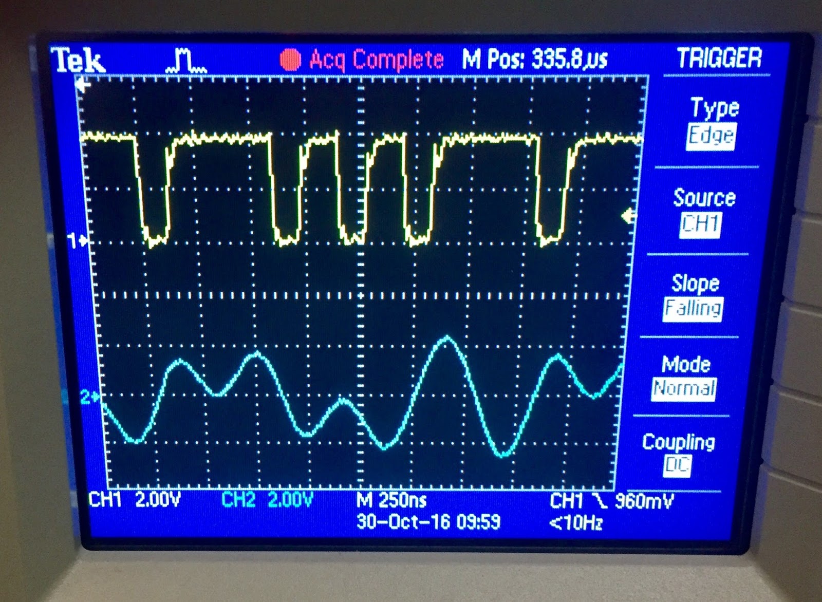
I did some tests using the logic analyzer trigger output to trigger the scope - looking at SectorMark at the time that I received the gotsector signal. They were essentially at the same time, except for a few 20 ns cycles used by my matching logic. As long as this is the correct sector number, I am beginning to write at precisely the proper place - the beginning of a sector.

Next up, I triggered the scope at the same gotsector point, advanced to the time when the sync bit would be emitted to start the label record, and did see that transition, both on the logic analyzer and by reading from the differential amplifier inside the drive via test point 1.

The odd dip of the signal is occurring when writing, which definitely causes the data separator to be confused and return junk. I still don't have official statements about the validity of the ReadClock and ReadData signals when writing, only innuendo from comments in Alto design documents, ergo I can't clearly flag this as a flaw.
Reflected write signal showing sync word 1 bit is 2 us to right of center, but also notice dips
I did see an anomaly - the bits being written for the label record are not correct - I see the first four bits of the data word going out as '1' but the intended content is not that. I can't double check the word showing in the logic analyzer against this because I am only emitting the low 8 bits of the word. I do see what appears to be an incorrect memory address, so I will look there.

I will also emit the sector number so that I can check it against the gotsector signal, since I am going through the investment of a 30 minute cycle to generate the new bitstream with high data word and sector number signals.

Testing with the new signals and the modified logic analyzer formatting showed me two things right away. First, the sector number is indeed 0000 when gotsector fires, which is what it should be. Second, the fetched word to serialize is incorrect. Not sure why, but time to zoom in one the memory access as part of the WriteField process.

Time to look for race hazards or timing errors in my use of the memory access FSM. Another half hour of idling about until I could watch the signals I selected - bits 16 down to 1 of the memory address and the low order three bits of the fetched data word. I can easily check this against the contents of RAM which I can fetch through my USB link transactions.

It appears that it is a timing issue, which I hope I corrected by adding one extra cycle before loading the serializer with the output of the RAM access. I also switched the instrumentation to show the full output data word from memory.

It appears I am writing the contents correctly now - verified at least through the header and label records - but the checksum that is written out by WriteSector is not valid when doing a ReadSector. This is undoubtedly also a timing issue that just needs a bit of adjustment to get right.

As I suspected, the signals from testpoint 1 are clean, with no dips in the middle, when doing a read. Similarly, the separated data bits are clean and correct. This tells me that at least with this drive, it is not possible to 'loop back' the ReadClock and ReadData to check what is being written.

Testpoint 1 while reading - sync bit 1 to left of center and first word x7900

ReadData bits corresponding to signal above - good data separation
I am fairly certain I found the problem. It is a classic mistake where a clocked process in VHDL is coded as if it were sequential - like programming - when in fact all changes to signals only take place at the next clock edge.

I updated the checksum by XORing the last word of the record, then later output the checksum as the next output word for the serializer. Sounds correct, but in fact the latter step will use the old value of the checksum, prior to the XOR. Thus we leave off the value of the last word from the checksum.

The change was made, as well as displaying the running checksum on the logic analyzer - after the obligatory 30 minutes of processing - and I tested again. First I run a WriteSector and observe the checksums generated and written by the logic. If that passes, I will switch over and test a ReadSector.

As a means of testing checksum generation, I built a little spreadsheet and used that with the label record value of the real sector 0 I am trying to write. The checksum should be x7CF3 if it includes all eight words of the record.
My spreadsheet to calculate checksum values for records
This explains why the ReadSector validated the checksum of the header record but rejected the label and data records. The contents of the two words of this header are 0000 and 0000, which produce the same checksum whether I drop the last word or not. XOR by 0000 leaves the checksum unchanged.

When the new bitstream was ready, I set up the testbed and ran my WriteSector. The checksums were correct. When I ran the ReadSector, it completed with no checksum errors on any of the three records. I dumped the RAM up to the PC and validated that it was a word for word copy of what I tranferred down to RAM to write to sector 0.

I will call it a day - nice success point in the testing so I leave the testing on a high. Next up is to adapt or write a program so that I can easily set up all the sectors of cylinder 0, which had been inadvertently erased, into the RAM allowing me to restore all of cylinder 0 to the contents found in the xmsmall.dsk archive that matched this cartridge. 

Digging into what is on the disk surface, what I read and what I wrote

ALTO DISK TOOL

I happened to set up the scope to trigger on SectorMark and show the incoming stream from the disk heads at various delays afterwards. I noticed that most of the stream was the unmagnetized, essentially erased noise signal but there are patches with strong clock and data modulation.

I then did single shot traces, which would mostly give me noise but sometimes would hit a sector with the good data. Digging through that data showed me that I have a major timing problem with my WriteSector process.

The noise ran for about 240 microseconds then the disk surface had strong clear disk clock transitions. I forwarded almost 35 word times ahead to where it should be writing the sync word and header record, where I found some 1 bits modulated between the clock pulses.

I should be erasing almost immediately after the SectorMark and clock transitions should begin within 2 us afterwards. Something is clearly wrong with my logic, which is all correct from issuing WriteGate/EraseGate onwards but the time that these are first asserted is garbage I guess.

Interestingly, I had very good extraction of the 1 bits and conversely no false bits extracted during the long preamble time where data is always 0 valued. Things are looking up, in an odd way. It does appear that if I can figure out how my WriteSector is malfunctioning and fix it, I should be able to write properly.

Time to go back to my logic analyzer trace of the WriteSector process, but begin the triggering at the rise of SectorMark to give me good timings for when the state machines are transitioning. To do this, I need to change the instrumentation on the fpga to emit those signals.

To reduce the amount of erased junk on the surface, I did a WriteSector of all 12 sectors on cylinder 0 head 0, which I confirmed by running the scope free and watching the signal from the heads. At least I know that the drive is capable of writing clock and data signals.

Working mostly with the scope at first, I triggered on IndexMarker and delayed far enough to be into sector 0. The first 1 bit, for the sync word, seemed to be properly placed inside the sector. Whether the remainder is well formed, correct and in its place will require slow careful examination. 

Monday, October 31, 2016

Still trying to find cause of failure to write

ALTO DISK TOOL

Some conditions are tested for by the circuitry in the Diablo and would result in a WriteCheck condition:

  • WriteGate on but no write current
  • Head current when WriteGate is off
  • No Erase current when EraseGate on
  • Erase current when EraseGate off
  • Erase current through both heads at same time
  • Write current through both heads at same time
  • Voltage dips below 13.5 V


Presumably, my problems in the Diablo drive don't include those situations, or I would have an immediate WriteCheck. I do have the sporadic situation where the drive powers down, flashing both FileReady and ReadyToSeek/Read/Write signals a couple of times. 

To recap some other symptoms observed so far:

As noted yesterday, the voltage on the center tap of the upper head should be about +1V when selected, -1V when not the selected head and +14V when writing. I confirmed both -1 and 14V levels, but the selected level is noiselike at dozens of millivolts rather than roughly 1V. 

Also noted yesterday, when I measure the output of the differential amplifier responding to the read head output (testpoint 1 on the board), I see a dozens of millivolt noiselike signal when reading the sectors on cylinder 0, even after I write, but I get multivolt wide swings on any other cylinder. 

When I write sector 0, I see the WriteGate activate and the proper pulses delivered to the WriteData&Clock line on the terminator. Reading back the sector still has the essentially erased output, millivolt noise, but no signal swings.

Therefore I need to check step by step to verify that my write signal is delivered to the heads properly. It would be easy if I had an extender card to push card J10 back giving me direct access to the various probing points, but to use it I would also need an extender for the cable from the read/write heads. Don't have either.

First new observation - I set the scope to trigger on the WriteData&Clock signal coming from the fpga and put the other probe on testpoint 1 to observe the flux reversals. I saw an odd dip in the midst of each transition, and the pattern for when I had a 1 bit wasn't correct either. 
Top line shows flux reversals I should see on testpoint 1


Test point 1 with odd decay in each signal


Clipped signal at TP2 seems almost the reverse of what I should see - dips when bit is 0
I am writing multiplexed pulses correctly, but write current might be wrong

The testpoint 1 is at one output of the differential amplifier on the read head. The trace without the dips would be seen when reading this sector. Since the Alto docs mention leaving ReadGate on during a write and observing the written bit stream, I presume that the testpoint 1 signal should look legitimate, without the dips. The dips are bound to cause false recognition of both clock and data bits. 

Here is the sequence of observations that must be made to determine from where the malfunction stems:
  1. Scope on output of the D flipflop that causes flux reversals, triggered by WriteData&Clock
  2. Scope on inverse output of the D flipflop  triggered by WriteData&Clock
  3. Scope on head bus A, triggered by WriteData&Clock
  4. Scope on head bus B, triggered by WriteData&Clock
  5. Scope lower surface head to verify its +1, -1 and +14V behavior

I set up for test 1 and 2, putting micrograbbers on the flipflop pins. Both sides of the flipflop show transitions just as expected. I have labeled these A and B respectively in the closeup of the schematic below.
Testing at Q and notQ output of D flipflop

Expected signal at point B (notQ)
Signal at point A (Q)

Next up is to scope on head bus A and again on head bus B. The bus A signal looked reasonable, although it only swung down to +5V from +14, not sure if that is correct. On to look at head bus B to compare. 

Head bus A signal
The other bus looked similar, evincing swings from 5V upwards, but I can see that the upper half of the bus A waveform is clipped off compared to the bus B version. I will now look at the bus A path for components that might cause this distortion. B is nicely symmetric while A is not. 

Head bus B signal

The above two views of bus A and bus B are taken from points C and D of the schematic excerpt below. Next I moved over to points A and B to see the drivers of the two bus lines.

Probe spots for head bus A and B

The signals at points A and B above both look good, equally symmetric. Whatever is clipping the peaks of the signal at point C (my Head bus A signal above the schematic) occurs on the right hand side of diode B81. 

point C - bus A driver
point D - bus B driver

Now, I move to figure out what is clipping the tops of the bus A signals once it moves through the diode D81 I will repeat the view of points A and C, the ones that showed clipping, but while writing on the lower surface (head 1). This will eliminate the head itself as a causative agent. 

I ran the tests and saw no clipping on the head bus A or B when writing on head 1. I then switched back to head 0 (the upper surface) and captured bus A again. Now I am confused - this time I saw no clipping. 
Retest of point C on upper head - this time no clipping

Still, once the sector was written, when I tried to read it back the signal was like noise, not the magnetization level I would expect. At this point, I am still mystified. 

Musings - could the voltage swing on the bus be too small to flip magnetic domains? Seems unlikely given how symmetric the behavior is. Is something wrong with the erase winding or driver? 

One final test of the evening - monitoring the erase driver input to the drive transistor, just to be certain that it thinks it should fire. I suppose one cause for the lack of discernable transitions when reading is that the write is actually not doing an erase, thus layering so many transitions that there is no clear signal to read. 
Probing point to check erase operation

Erase driver definitely turning on

Now that I see the drive voltage firing up for the erase driver, and had previously seen a current draw curve that was similar to this, I have to again assume that erasing is working properly. I remain mystified as to what is happening on the drive. 

Oddly, after I write the sector, I see checksum errors on the label and data record, but not header record when I try to read it back. Since the write is producing its own checksums, that is definitely odd.