Friday, August 5, 2022

Feeling good about generating a read head stream of pulses but not done yet

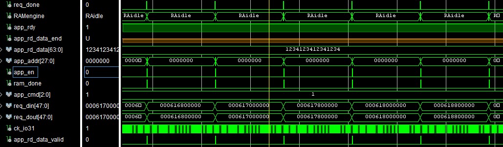
IMPROVED FAKE MEMORY MODULE TO SEQUENCE VARIOUS DATA WORDS

I made changes to the fake memory module such that it would produce a known stream of word values that appear to be the data read out of RAM. Eight values were chosen with an eye to validate that words are produced correctly and that the first and last bits of adjacent words are not corrupted due to poor timing of the read results.

TIMING IMPROVED TO ENSURE THE NEXT RAM VALUE IS FETCHED BEFORE EACH WORD

I had to find a way to trigger the read of RAM late in the bit generation of a word in order to have the data available for the next word to start its output. Since the last four bit cells are a check word whose value is already calculated after finishing the 16th data bit, I could issue the trigger at this point with no consequence for when the RAM result is latched in. 

That new value from RAM can appear anytime from the start of the first check bit all the way to the beginning of the first data bit of the next word. The first value from RAM has to appear before word 0 starts its generation, thus I found a time during the latter part of the sync word output where I could trigger the read. Since sync is a fixed pattern, it does not matter when the RAM data arrives as long as it is by the time word 0 begins. 

CLOSE STUDY OF BIT GENERATION DONE

To assist with this study, I emitted a pulse at the start of each bit cell, which should neatly delineate the pulse or pulse pair that are a 0 or a 1 value. It also allows me to visually look for incorrect duration of bit cells. Coupling this with the edges when the word number changes and I had all the tools I needed to verify that my circuit was operating as intended.

I did find a number of suboptimal situations which I am working through. Adjusting here and there. Hopefully I will be happy tomorrow and ready to move on to capturing sector writes. 


Thursday, August 4, 2022

Substituted fake memory module for the real memory interface - speeding debugging

INSTANTIATING A MODULE WITH THE SAME INPUT OUTPUT BUT MINIMAL LOGIC

I took the interface design of the memory controller module and used that to build a false memory module. It was easy to stick that into my design, although I did have to drive a few signals and provide the clock that the rest of the system depends upon. 

A clock module was built into the fake memory module to provide the 50MHz main clock for my FPGA logic and I forced the app_rdy signal high to indicate that the controller is ready for commands. I then worked up a delayed response to signal that the data was available from the RAM read, sending the data valid signal four cycles later to ensure that my driving logic is sound.

SPEEDUP IN SIMULATION SPEED, MORE THAN 10X FASTER

My VHDL is simulating much more rapidly now that it isn't trying to represent all the gates inside a memory controller. I believe it is at least ten times faster, perhaps as much as 15 times faster, which makes a simulation run bearable as I iterate testing and repairing my logic. 

WORKING MY WAY THROUGH THE READ REQUESTS UP TO THE RAM MODULE

The high level flow of my logic is that as we begin on the next word being read in a sector, we push a 48 bit request that contains the address in the RAM and a bit that requests a read (16 bits are unused for reads but contain new data on a write). 

The FIFO that has had the request inserted alerts the FIFO emptying process to pull the request, which then triggers the RAM engine. I correctly set up the addresses, the read command byte and the enable flag for the two cycles needed to cause the memory controller to begin a read. Several cycles later the RAM has completed the read and turns on the ram_done flag.

At this point, the response FIFO filling process would package up the word just returned and push it into the queue. The FIFO emptying process will load that content into the active word register which is used to shift out the 16 bit cells plus the four check bit cells. 

I verified up to the activation of ram_done at the proper point. Tomorrow I will watch the response FIFO work and check to see whether the new word is in place fast enough for the generation of the first bit cell.

Triggering the RAM engine to read each word


Quick update on simulating DDR3 memory interface

SIMULATION MODELING PROVIDED ONLY FOR VERILOG

The models that will accurately simulate the DDR3 memory interface I generated and permit me to verify that my driving logic is correct were built for Verilog based projects. Very approximately you can talk about hardware description languages as being in two camps. The government established VHDL as a standard and toolmakers support this language in order to participate in the funds that flow from defense projects. Various toolmakers promote an alternative, Verilog. 

Xilinx is a toolmaker. Many hardware device makers are also aligned with the Verilog camp. The result is that the only simulation models that can be used for the DDR3 memory in the Xilinx toolchain are based on Verilog. 

The simulation models have a handy parameter - SIM_BYPASS_INITIAL_CAL - which will turn off the modeling of the lengthy process by which the memory controller has to write and check all bits in order to adjust timings for the most reliable operation, as part of its initialization. This process is cumbersome and not practical for simulations, so they provide options such as FAST and NONE to speed up this stage and allow the designer to focus on their interaction with the memory controller and not on how the chips work internally.

This sounds great, but there is no method I can discover, either by myself or on the interwebs, where a VHDL based memory interface can access that parameter to modify it. Were I to have written the project in Verilog and implemented the memory interface in Verilog, I would be merrily debugging. But No! Not for you, lowly VHDL oriented designer.

Time to devise a workaround - either a dummy module to substitute for the memory or some other convoluted hacking of my code - since I really need to see waveforms to be comfortable that my read and write requests are set up properly. They have to happen in the right dance of interlocking signals, occur at the correct timing and with all the necessary setup and hold timing so that the memory will work properly. 

More learning curve - memory interface generator, DDR3 memory and FIFO startup requirements

SIMULATION SHOWED FIFO BEGIN FULL

When I begin my debugging of the RAM access mechanisms that would be driven by the disk modeling to fetch words of cartridge data, I saw that the FIFO is marked full at startup, which blocks me from pushing in any requests for RAM access.

The reset of the FIFO should result in the flag being off so that I can write a request into the queue. I began monitoring all the signals involved in the FIFO and the reset logic, where I saw the flag sitting at full. Some investigation shows that the reset of the FIFO must occur after its clocks are operating in order to properly reset. Perhaps when my power on reset is asserted the clocks weren't running, so I planned for a FIFO reset signal that would blip on for a few cycles well after my reset is complete.

IMPLEMENTED RESET LOGIC FOR FIFO BUT STILL BLOCKED

The FIFO reset was generated as I expected but I still didn't see the full flag go off. Tracking the clock produced by the memory interface circuits that is used to empty the request FIFO and feed the response FIFO was illuminating - no clock coming out of the memory interface. 

A bit of reading highlighted the need for the interface to complete calibration before the DDR3 memory is ready for access, said completion to be signaled by a calibration complete signal out of the memory interface. I set up a run to watch for the completion signal and the appearance of my FIFO clock. 

DDR MEMORY INTERFACE CALIBRATION WAIT 

I ran the simulation for almost half a second but never saw the calibration complete nor the clock begin operating. This led me to look closer at the reset for the memory interface generator. It was active low - thus I had to invert my usual power on reset signal to cause the memory to be properly reset. 

Once the memory interface was properly initialized and the FIFOs were ready, the number of changing signals that had to be simulated shot way way up. The speed of simulation slowed to a crawl, from its already pokey rate.  A quick estimate was .2 milliseconds of simulation for each elapsed minute. 

To see the signals I care about I think I need to get to around 25 milliseconds total time in the simulation. That means something in the vicinity of 125 minutes to reach that point. Yikes - the investigations are going to be painful if every small insight requires 2 or more hours to check out once the issue is resolved. 

EXAMINATION OF RAM REQUEST PERFORMANCE DURING SIMULATION

After waiting several hours I was able to see that at least my front end of the RAM access mechanism is working. I saw the trigger cause the request to be pushed into the FIFO, it was then pulled by the RAM engine and that engine advanced to the next step of its state machine. Unfortunately, it did not proceed any further and that meant we would not generate the ram_done signal to push a response into the second FIFO. 

Looking at the logic it was immediately apparent that the problem was that the memory interface was not activating its interface app_rdy signal to indicate it was ready to accept commands. This was consistent with the initial calibration completion signal remaining off. 

I need to look very closely at how to get the memory to simulate through to a completion of calibration as that is an essential prerequisite to the interface becoming ready for operation. Since each attempt to verify a fix will take more than two hours, I have to be more careful and complete in my studying to avoid wasting huge portions of a day. 

One way I can shorten the wait is to fast track the disk rotational model - right now it starts with a SM, then a SM + IM, after which it takes two more SM before it can begin to request data. Each SM interval is 5 milliseconds, so that burns 20 milliseconds when no useful information is being collected. I will start the testbench for simulation at the index mark, this should cut the delay about in half. 

I will also be looking at a parameter for the memory interface which will produce a fast calibration during simulation - hopefully that will make the memory interface happy. 


Wednesday, August 3, 2022

Bitstream generation and disk modelling verified through simulation

THE MECHANICS OF A SECTOR ON THE DISK DRIVE

As you remember from prior posts, each bit written on the disk is an approximately 1.4 microsecond interval called a bit cell which is divided into two halves that can record a pulse by switching the magnetic field direction. No switch means nothing is written and nothing is detected by the read head.

The first half provides the clock and the second half has a pulse if the data value is '1', while if it is absent we impute a data value of '0'. There is always a pulse in the clock half of the bit cell, this is how the drive achieves self-clocking.  A long train of words of all zero provides nothing but the clock pulses and trains a data separator to recognize which is the clock half and which is the data half, so that the pulses can be separated and sent out their own clock and data signal lines. 

Thus, we need to have a way of training the data separator and that is achieved by a fixed format for the sector. Each sector begins with a sector marker, a pulse that is 160 us long. Having masked every other physical sector marker, we see only four of the eight and that defines the four sectors following the index marker pulse. 

At the falling edge of the sector marker pulse, we begin writing all zeroes, a clock pulse followed by no pulse in each bit cell. This is produced by the IBM 1130 device controller circuits for 250 microseconds, after which a sync word is written. This is a word whose high order bit is 1 - 0x8000 - with its proper error checking bits. Immediately after this sync word of twenty bit cells is written the device controller commences writing the 321 words that fill this sector. 

Each word of 16 bits from the CPU is augmented with four error checking bits at the end to yield 20 bit cells going onto the disk. The bits stream onto the platter from the low order bit up to the high order bit then the four check bits are written. There is no delimiter between words, we have only a continual stream of bit cells and depend on the device controller logic to break them into words of 20 bit cells and then data words of 16 bits going to the computer. 

From the moment the sector marker pulse trailing edge is seen, we have a stream of about 6,620 bit cells must be divided into 321 words of 20 bits each. The sync word pattern following the stream of about 180 zero bits allows us to know that the very next bit cell is the low order bit of word 1 and that every 20 bit cells thereafter is the low order bit of the next word until we have read or written all 321 words.

A sector is nominally 10 milliseconds long at the 1500 RPM rotation speed of the disk platter, minus the 160 microsecond duration of the sector marker pulse. Our pattern of zeroes, sync word and 321 data words burns up about 9, 268 microseconds of the 9,840 us available on a sector. We need some safety buffer because the disk rotation speed can vary in the real world,  the physical slot that produces the sector marker might be inaccurate, the length of the generated sector marker pulse can vary, plus the oscillators generating the bit cells can vary a bit. 

In an ideal world we could have fit another 20 words into the sector but if the sector marker pulse rises before we have processed the last bits of the sector we generate an overrun error and have to abort the read or write.  

MY LOGIC IS TRACKING THE DISK ROTATION VIA THE SECTOR AND INDEX MARKERS

Upon startup, I wait until the platter has rotated to an index marker, which sets up my logic (and sets up the IBM 1130 device controller logic) to treat the next sector marker as the beginning of sector 0. I block any bit cell generation until I have encountered the index marker.

The sector modelling logic is triggered by the sector marker, beginning to write bit cells of data value '0' after the fall of the sector marker pulse and continuing for 250 microseconds. It then writes the 20 bit sync word pattern B00000000000000011110 which is x8000 with the proper error checking bits.

I then write successive words as 20 bit cells, counting the words as I go. Each time a new word starts, a read request is pushed into the FIFO queue for the RAM with the address corresponding the cylinder where the arm is sitting, the head selected, the current sector number, and the word number. 

I use the returned word from the RAM response FIFO to shift out the 16 data bits, bit position 15 first and continuing leftward until we get to bit position 0 at the high order end. As each bit is written, any '1' value bits are added to a running counter. When we have finished with the 16 bits of the data word we produce the appropriate four check bits based on the running counter value. 

As previously mentioned, the purpose of the four final bits is to detect errors. The more obvious way it does this is by sending 1 bits until the total of all 1 valued bit cells is evenly divisible by four. Depending on the number of '1' bits in the data word itself, there can be 0, 1, 2 or 3 additional '1' bits that must be written. The device controller verifies that the full 20 bits read in have '1' bits that are 0 modulo 4 and throws up an error if this isn't true.

The second and less obvious error checking, not implemented in the IBM 1130 but possible due to this error checking scheme is to validate that the last bit written is a '0' value. It must always be '0' because the controller of the IBM 1130 writes either B0000, B1000, B1100 or B1110 to make the 1 bits a multiple of four. Three bits are sufficient to accomplish this, thus the fixed fourth bit of 0 is another kind of error checking and may play a role in ensuring that the data separator remains able to distinguish which pulses are clock and which are a 1 data value. 

At the end of the day, I had simulator runs showing me that the stream of bits were produce exactly to this schema and at a realistic timing that matches what a real world cartridge would produce through the head. I had a signal whose level varied beween +3V and 0 to feed to the disk drive electronics at a specific point. 

The drive spots magnetic flux reversals, converts them to one polarity regardless of the way the flux swings and from that produces a pulse for a reversal. The pulse is turned into a transition of a logic signal from 1 down to 0 for the length of the pulse. Thus, my signal stream is interpreted at this point as a pulse for as long as the level is 0 and absence of pulse all the time is stays up a +3V. 

The duration of my pulses are set to 0.4 microseconds which fits within the 0.7 us bit cell half and enough separation between the timing of the clock and the data pulses to be properly separated. 

There is an esoteric effect on disk drives where the timing of the pulse detected 'shifts' based on surrounding flux reversals. The separator has to accommodate this time shifting without errors. I don't think I have to shift my own pulses but would be prepared to add this in if it becomes necessary.

SOME SIMULATION OUTPUTS

Sector spanning view
The section above shows more than one sector, so that you see the sector number change and the bottom stream of pulses that are the 6,620 bit cells produced for the sector. The top line is the sector number, the next down is the word counter. The two lines between the pulse stream and the word count are the state machines involved in sector modeling and bit cell generation. 

Beginning of a sector 
I have zoomed in a bit to show you some detail in the state machine and word counter values plus the pulse stream begins to show distinct patterns as the data bit values change. 

Bit cells visible

This final screen shows more detail so that the 20 bit cells of the sync word and bit cells of data words can be discerned. For this testing I produced a fixed word value of x5AA7 for each of the data words, which you can verify by decoding the bit cells and validate the check bits are correct.  

NEXT STEPS IN VALIDATION

All of the above depends on the RAM having returned the proper word in time for my bit generation circuitry to turn it into bit cells. The request for the word is generated just before we begin writing the clock pulse of the bit cell. We have 35 FPGA cycles for that half of the bit cell and then 8 cycles into the next half before the data value must be present. 

The RAM itself will return the data word in about four FPGA cycles, but we also have to traverse a FIFO for the request and then a FIFO to pass back the answer - these take a few cycles each. On paper I have enough time since the RAM is doing nothing except serving up our word read requests. 

The reason for the FIFOs, by the way, is to deal with the different clocks involved. The DDR3 RAM operates with 100MHz and 200MHz clocks, while my logic is running at 50MHz and that is not exactly in phase with the clocks of the RAM. 

The FIFO is implemented to act as a buffer to accommodate the dual clock domains, one on each side of the FIFO. It will have either zero or one item in the queue at any time, not really storing up a queue of requests. One FIFO from 50MHz to 100MHZ for requests and then a second FIFO for responses from 100MHz back to 50MHz. 

I won't have real data in the RAM during the simulation, but I can validate that all the triggering takes place. My sector modeling logic must trigger a request into the request FIFO before each word, the RAM side must see the request and pull it off successfully, and the data must be set up to read the RAM.

I then have to watch the state machine driving the RAM to see if it seems to toggle the control, address and data lines at the proper times. Assuming that is good, then when I see the signal from RAM that data is valid, I must see the data pushed into the response FIFO and my logic pull it out on the far end to put it into the word buffer for the bit generation circuitry. 

Once I get through all this checking, then if the data is able to be written into the RAM prior to disk operation, I will have some confidence that the disk drive electronics will be seeing the right stream of pulses to turn that into 321 words for the CPU. 

Tuesday, August 2, 2022

Finishing the drive modeling and simulating as I go

ARM MOVEMENT MODELING FULLY TESTED

I put the logic through its paces with simulation to ensure that I will properly capture the position of the arm (cylinder number) at all times. During the course of this work I discovered a signal I need to capture that I had not built into the original plan. This is +Access Ready which goes low then back high for each arm movement. With that signal I can properly interlock my logic to ensure I capture exactly the right number of moves. 

BUILDING LOGIC TO PULL WORDS FROM RAM AND EMIT BITS TO THE DRIVE

As the rotational model reaches the time when each word of the 321 words in a sector is complete, it bumps the word counter and that serves as my signal to fetch the next word from RAM so that it can be fed bit by bit to the drive circuits that process the read head signals. 

From the time I see the bump occur to the next word, I emit the 16 bits of the data word, with the low order bit output first and moving sequentially up to the high order bit 0. Each bit of the data word is sent with a 1 pulse during the first 700ns and then the value of the bit as a pulse in the second 700ns interval. Together the 1.4us represents one bit cell on disk as either a pair of bits or a bit plus an absence of a bit. 

In addition to the 16 bits of data I am writing in the 16 bit cells, there are four check bits sent at the end of each word. The error checking scheme is to have the number of 1 bits be evenly divisible by four. Thus, depending on the count of 1 bits in the word itself, we write 0000, 1000, 1100 or 1110 as the last four bit cells. 

SKETCHING OUT CAPTURE OF WRITTEN DATA

Capturing the data involves detecting when the CPU believes it is emitting a clock bit and when it is sending a data bit, so that I can assemble these into a word then push it into RAM. To do this, I realized I may need both clock signals the drive is generating for writing - phase A for the clock bit and phase B for the data bit. I added the phase A which was not in my original plans.  When WriteGate is activated, the drive begins to emit the clock signals and writes the clock pulse and the data 1 bits to the surface immediately. The scheme for encoding bit cells is to have the two phases, A and B. A flip of the magnetic field is always written during the A phase,  but a flip is only done in the B phase if the data value is a 1. If the data value is 0, nothing happens on the disk surface. 

This makes it impossible to recognize when zero bits are being written other than to see the clock bits (A phase) and note the absence of a pulse for data. Having the two clock phases in my circuit ensures I will know for certain what pattern of bits is being written onto the disk surface.

Since, however, the heads are not loaded on the disk surface, we have to capture the bits and update RAM to keep our virtual cartridge reflecting what input-output has taken place. Writing the word to RAM will take place after the 20 bits have been captured coming from the CPU, whereas my reading logic reads the word from RAM before it begins streaming the 20 bits to the CPU. 

This implies that my state machines must issue RAM access requests at different times for read versus write. There is a similar duality with the SPI link between this FPGA and the Arduino - data downloaded from the SD card file to the RAM is captured at the end of a word transaction on SPI, while uploading changed content from the RAM back to the Arduino has to set up the word before the word transaction begins. 

Validation of drive modeling in FPGA by simulation is well underway

TWO OF DRIVE MODELING READY TO DEBUG

In order to inject the proper bits into the read circuitry of the physical drive or to snag written bits to update my virtual cartridge, I have to model the position of the read/write head very precisely. This involves two dimensions of movement - radial and rotational. 

The radial modeling captures which of the 203 cylinder locations the arm might be positioned at. This involves sensing some feedback signals and capturing the control signals which cause the arm to move in or out. 

When the arm is fully retracted to the location of cylinder zero, the home cylinder, there is a microswitch that activates and generates the +Home signal. As the arm moves, it turns off the +Access Ready signal until it is settled into its target cylinder position. 

The drive is given a direction of movement and a step size. The arm can move towards the home cylinder or out towards cylinder 203, depending upon the direction signal. Movement takes place in either two cylinder or one cylinder steps per movement request, controlled by the 10mil/20mil signal. Whenever the Access Go signal is seen, the mechanism moves according to the direction and step size.

My logic tracks the cylinder by accumulating the various movements, such that I should always know where the arm is positioned on the real drive. 

The disk surface is rotating continually under the heads. The disk drive picks up sector mark and index mark pulses to know what part of the circular path is under the head at any instant. My modeling is following the rotation of the real cartridge so that my virtual cartridge can access the data word associated with that spot.

A comparatively trivial part of the modeling is to watch two signals. One, the track signal, selects either the bottom or the top head on the arm since data is recorded on both surfaces of the physical platter in the cartridge. The other is the control that keeps the heads loaded on the physical cartridge and the disk drive ready for access. I don't allow the drive to actually load the heads into contact with the platter but I keep track of the signal. When it switches off, we must stop simulating disk read or write activities. 

There is a complication because the physical cartridge has eight sector marks evenly distributed around the platter, each providing an approximately 160 us pulse. In addition, there is one index mark that occurs shortly after one of the sector marks, which defines the 'start' of the track. The IBM 1130 instead treats the disk as having four equally spaced sector marks, which it accomplishes by blocking every other sector mark during operation. 

My circuitry sees the eight SM and one IM signals, at all times generating the sector number where the head is currently passing. This is used as part of the RAM addressing for the current word, which is an amalgam of the cylinder number, top or bottom head (track), sector number and then which of the 321 words in the sector is under the head. 

A related part of the circuitry has to model the sector in detail. As each sector begins, at the falling edge of the SM pulse, we will have 250 us of zero bits, a specific pattern which is the sync word, then 321 words of 20 bits before we pad the remainder of the sector with zero bits again. My circuit times from the sector mark and moves a state machine through the stages - zero bits, sync word, the 321 data words and final zeros. It generates the word number at the proper time to match what the real cartridge would have passing under the head

STATUS TO DATE

The head (track) selection and head loading signals worked properly. I moved on to the rotational modeling, which is now clearly working as it should. I see the stages in a sector occur at the proper time and the word number increment every 28 us which is a valid timing for a 20 bit word. The entire sector of 321 words fits nicely in the sector with a bit of zero word padding at the end. 

The sector numbers are generated correctly and synchronize properly based on the first index mark pulse received. The programmer issues an IO command which includes a two bit sector number. The drive controller logic in the CPU watches the SM and IM pulses to track the sector coming up, beginning input output operations at the sector mark after an equal compare of target and actual sector numbers. 

The cylinder movement engine is still getting some tweaking, to ensure that I properly interlock to always count the same number of steps as the real arm traverses. There are subtleties - behavior when the arm attempts to move inward past cylinder 202 or outward past the home cylinder. The mechanism reports a successful movement but in fact the arm stops either at home (0) or 202. The +Home signal helps detect this on the cylinder 0 side, but no feedback exists to indicate this for movement attempts beyond 202. 

I should be able to finalize the operation of the arm movement modeling tomorrow and move on to the coding and testing of the bit generation itself - the delivery of the 16 bits of a data word in the proper order and the subsequent four check bits that provide error checking. These have to be timed to coincide with the data separator in the disk drive.

The separator will entrain on the long sequence of zero bits at the start of the sector - a word of all zeros consists of alternating 1 and 0 bits which are the clock and data respectively. This is cemented by the sync word pattern so that the drive is now diving each bit cell into two phases - A and B - that represent the clock bit and the data bit. 

When phase B is active we either inject a bit if the data value is 1 or stay inactive to assert that the bit is 0. Thus, my logic watches the 700KC B signal to time when it produces the raw data stream. We always inject a 1 bit when in the midst of phase A then selectively inject the bit in B based on the data value.