Sunday, November 30, 2014

Installed new drive belt on 1053 console printer

1053 CONSOLE PRINTER RESTORATION

Due to the rain, spent time inside the garage working on disassembly of the cycle shaft in order to replace the motor drive belt on the console printer. By 9:30 AM I had the new belt in place, with the cycle shaft hanging loose in the frame. Reassembly should not be not much harder, but then comes all the adjustments that now must be made since I had to disturb so many settings with the removal.
Removing various parts in order to move the cycle clutch shaft
Cycle Clutch shaft pulled to left, allowing access for new belt

The pulley in the middle is where the drive belt is installed
New drive belt installed but shaft not yet reassembled
By mid afternoon it was reassembled but not yet adjusted. Later I have to adjust:

  • backlash on gears
  • lateral play on cycle clutch latch (should not have changed)
  • cycle clutch latch height (although I didn't unfasten it)
  • cycle clutch spring angular position (timing of clutch release)
  • filter shaft timing relative to cycle clutch shaft
  • print shaft timing relative to cycle clutch shaft
  • C2 contact timing (feedback to 1131 while the print mechanism is busy)
I am off early tomorrow morning on a trip to Las Vegas, returning Friday evening and will be celebrating my wife's birthday tonight as I will be out of town on the actual birthday. No more work on the physical system until Saturday but I will haul along the tools to continue writing code for the FPGA and for the PC side software, in any free moments I will have. I don't expect many as I am fully booked for the entire conference.


SAC INTERFACE FOR ADDING PERIPHERALS TO THE 1130

Lots of rain today, no chance to set up outside and continue with the wiring.

Saturday, November 29, 2014

Beginning console printer disassembly plus more wiring of the SAC Interface Box

Two impediments to working today - heavy rains and a road trip to visit a dog we might adopt. I did what I could inside the garage, turning to some mechanical rehabilitation that was reasonable while shut in.

Due to congestion in the garage, wiring and construction projects are easiest to do by setting up a long folding table just outside the front of the garage, with the door raised, but that won't be much possible with the heavy rain underway.

Instead, I will drive over two hours each way to meet with an owner of a dog my wife is considering adopting. Our family dog passed away a bit over a year ago and she feels it is time for another one to live with us. Back in the mid afternoon, I could then move into the garage for an abbreviated work day.
Kerry, the dog we hope to adopt
1053 CONSOLE PRINTER RESTORATION

I forced myself to sit through the entire video series (Selectric Training) on Youtube, hours long, to be sure I was ready to tackle the replacement of the drive belt on my 1053 console printer. The course was released as audio cassettes plus color slides, which someone has now combined into a series of videos and uploaded. The narrator speaks slowly, which gives the entire course a plodding feel, dragging along but with short bits of important information sprinkled throughout.

I took off the front panel and cover of the console printer and prepared to disassemble the cycle shaft. The first couple of steps involved removing the cover over the gear and taking off the degree wheel that rotates at the left side of that shaft.

Covers and front panel removed, ready to start surgery

The cycle shaft is the left 2/3 of the picture

SAC INTERFACE FOR ADDING PERIPHERALS TO THE 1130

The skies cleared up late in the afternoon allowing me to set up the table outside and get more completed on the interface box. I have the hybrid solid/stranded wires with the crimp pins installed for all the signals and have installed the 12 driver signals from board three into the fpga connector.

I accidentally installed two pins out of order but I will correct this by breaking the joint and swapping the stranded wires to the opposite solid wire. In this way, I don't have to extract the pins from the connector to move them to another spot. They stay in place but are hooked to a different wire to the interface board. There was no more daylight at this point so I had to stop the work.

I have five more driver pins to install into connectors, those hooked to board four. As well, I have the 12 receiver pins from board three to install before this wiring is complete.

Friday, November 28, 2014

More construction of SAC interface box

SAC INTERFACE FOR ADDING PERIPHERALS TO THE 1130

I got up and began working as soon as the sun was up enough to light my worktable in the garage, my top priority being to finish the interface board wiring to the 160 pin socket and to the connectors that will fit onto the fpga board assembly.

I found that the rigors of pushing in the pins to the connectors would often stress the solid wires I had used for the links, I decided I had to abandon those and replace them with thin stranded wires. I hate connectors,  which often become the most fragile part of my assemblies.

In this case, my decision to insert wires directly into a circuit board on one end and into crimp on pins for the other left me with a 'no win' scenario. Pushing multistrand wire through a PC board hole is an exercise in frustration, but using single conductor wire to the crimp connectors inevitably leads to the wire snapping off the connector after some degree of flexing.

The leads from the 160 pin socket to the board have the same issue, but one I optimized for ruggedness by using stranded wire on that side. I soldered a small section of solid wire to the end of one side to form a 'pin' I could push into a PCB hole and solder.

I will need to replace all the TTL signal wires with stranded wire, solder on solid 'pins' for the PCB side and crimp them on at the connector end. I realized I can use the ends of the existing solid wire, where they exit the PCB, as the 'pin' to avoid having to rework three boards times 24 leads each plus another five on the last board. Unsoldering, cleaning up and resoldering all that would have been a major pain.

Another task for the day was to select the mounting location for the FPGA board stack, drill the holes and mount it inside my enclosure. I made a paper guide for marking and drilling the bottom of the cabinet. The stack of two boards, FPGA and debugging/breakout,  is now mounted in place and ready for the connectors to be affixed.

FPGA board and breakout daughter card mounted inside enclosure
By 4PM, after working most of the day, I had the TTL side signal wires from the first two boards attached to the connectors and had begun on the third board. When the rest are hooked to the connectors, I have to tape up the soldered junctions between solid and stranded wires, dress everything up with cable ties, and then install the connectors onto the breakout board.

Separating interface boards while wiring them to fpga connectors
There is too much to do in the remaining daylight, so I will move inside and work on coding. I am implementing the FPGA side basic link to communicate with a PC (and also have to write the software to run on a PC.) The Visual Studio support for Python looks solid and I should have no problems using accessing the Adept libraries by using the 'ctypes' package in Python.

Thursday, November 27, 2014

Completed SAC Interface 1130 side IO capability, working on PC side

I completed more logic definition during the long flight from London to Los Angeles and on the ground switching flights, but didn't arrive home until the evening. As a consequence, I didn't do any construction or hands on work in the garage that day and today is Thanksgiving so I only got out for a few minutes today.

SAC INTERFACE FOR ADDING PERIPHERALS TO THE 1130

I completed the functionality to support up to 20 devices with the SAC interface, each configurable on the following dimensions:
  • area code (device address)
  • XIO functions supported
  • Use of cycle steal
  • Interrupt level(s) used
  • Priority of devices for cycle stealing
I am building some black box modules that the synthesis tool will assume are producing real input signals and/or are consuming some of the signals I generate. If I didn't do this, the synthesizer would recognize when outputs weren't used, trimming away all the logic to create them, Similarly, if there is no input or it is a fixed value, logic is trimmed away or replaced by a constant output. 

Careful attention to the synthesis report and all its fussy warnings is a best practice for successful designs, as these warnings may show a flaw in the logic or a missing connection. Even when it is purely noise, a bit of modification to the source can remove most of them. In that way, any warnings that do arise as you make changes have a reasonable chance of flagging real issues. 

I did some work on the link to a PC, which provides data, control and status for an emulated peripheral, but still have some design decisions to make before it can be fully implemented. 
It will leverage the Digilent provided USB system using the async parallel port mode, a quick way to allow code on the PC to send or receive data from a pool of up to 256 one byte 'registers' which are whatever signals I need. These will be the data out and in buffers, plus status and control information, for each of the implemented peripherals.

The logic to transfer pairs of registers (16 bit entities to match the 1130 architecture) is in place in my VHDL, ready to be used for functions inside the interface. The first two I will implement are a cycle steal access to memory and a display/update of SAC interface signals.

To create the PC side code, I set up Visual Studio Community, the free version of VS. I will use Python for my code unless I find some technical impediment to using the Digilent Adept software with that language.

I received the FMC Carrier S6 FPGA board, the Xilinx breakout board that attaches to it, and the parts for the plugs to connect my signals to the breakout board. In addition, I picked up a set of HP standalone probes - a logic probe, a logic pulse injector, and a current probe - that will be handy to identify which of the many drivers of a wired bus is driving the output to 1.

Monday, November 24, 2014

Basic IO functionality implemented for SAC interface

I am still in London and quite busy at our conference but did get some time to build more of the logic for the SAC interface. Today (Tuesday) is the last day of the event and this evening I will move out to a hotel at Heathrow airport in order to have a later wakeup and shorter day traveling home tomorrow.

I should have some time to work on the VHDL tonight, waiting in the lounge for my flight to board and then on the aircraft flying home. I arrive home tomorrow evening just in time for the US Thanksgiving holiday and a few days with the 1130 before I fly off to the next venue.


SAC INTERFACE FOR ADDING PERIPHERALS TO THE 1130

I completed my logic for handling multiple devices simultaneously including prioritization of access to the cycle stealing function. I have a block of Unit Control Words (which is a term used in the 1130's era to set up devices on S/360 channels) in priority order with flags that control the use of cycle stealing and interrupts.

All the basic processor (software) initiated IO activities are handled, the seven types of IO commands that define the IOCC which an XIO instruction invokes. These are Sense ILSW, Sense DSW, Read, Write, Control, Initiate Read and Initiate Write.

One type is used during an interrupt handler routine to ask every device to raise its hand if it has a request to be serviced by this interrupt level. The devices have their assigned bit positions in the ILSW, so the result returned to the software has a logical OR of all the bits returned by various devices.

Another type is the Sense DSW which asks the specific addressed device for its status - receiving a word in the accumulator with assigned bit positions related to various status conditions. Another function of the Sense DSW command is to allow resetting of the condition that caused a request for interrupt - if the conditions aren't reset by turning on this bit, then when the interrupt handler exits it will immediately be reentered by the hardware.

Read and Write commands are a means to move one word between memory and a peripheral device. The sofware gives the memory address of the data as part of the IOCC.

Control is a command that is used to trigger various device actions, by setting or resetting various assigned bits in the IOCC. Examples include seeking the disk arm to a new cylinder or causing a printer to move down a line.

Initiate Read and Initiate Write are used with devices that leverage the cycle stealing capability of the 1130 - the XIO command provides an address of a memory area to the device, beginning with a word count and continuing with space to hold that many words of incoming or outgoing data. The Initiate commands end as soon as they pass on the word count address, with the device then using cycle stealing to fetch the word count and later to read or write words to the remaining area.

Cycle stealing is a mechanism where a device can request a special memory cycle where the device provides a memory address and either receives the contents of that location or provides data to be written into that location. There are certain constraints on when the memory cycle takes place but in general these can happen almost immediately as soon as the current memory cycle underway is complete.

Since some operations such as addition or shifting can take a variable number of basic clock cycles to complete, the wait for the cycle steal to be granted is variable. Further, a device on a higher priority cycle steal level will be serviced first, adding more possible delay. Since we are usually talking only a few microseconds wait, this is fast enough for all the peripherals used with the 1130.

The next major coding task for this device will be the protocol and link connecting the interface to a PC, allowing the PC to be the source or destination of data that will be 'read' or 'written' by the peripheral device we implement in the box. We can have a mix of real devices which are hooked to the box plus emulated devices which use the PC link. 

Saturday, November 22, 2014

Visits with 1130 and 360 restoration/replica building peers in the UK, plus development of fpga logic for the SAC interface


SAC INTERFACE FOR ADDING PERIPHERALS TO THE 1130

I threw in a few hours of coding on the FPGA, during the train ride from London up to Bletcheley and back plus a bit of time in my hotel room. I hope to have enough to begin testing when I get back and hook up the interface boards to the Xilinx breakout card and new fpga board.

At each step as I code it, I realize ways I can generalize the design a bit more. The goal is for this to be a flexible framework that can be used to

  • allow quick loading and dumping of core memory from a PC file
  • hold diagnostic programs that can be popped into memory
  • emulate card readers, punches, printers and disk drives using PC files
  • hook real peripherals to the 1130 implementing a missing IBM adapter (e,g, paper tape)
  • hook real peripherals to the 1130 emulating IBM device (e.g. DEC RK05 as 2310)
  • extend functionality of the 1130 via device interface (e.g. floating point math)

My 1130 system, the system at the museum in the UK, an 1130 system owned by Brian Knittel and Norm Aleks, and an as-yet unrestored 1130 owned by the MARCH retro computing society in New Jersey all have the SAC interface installed. Other 1130s that are restored or might be restored in the future might have the feature installed, but I don't know enough about those machines to know.

Each 1130 system with the SAC installed could make use of the SAC interface I am building either temporarily to aid in restoration/repairs, temporarily to load or capture software to exchange with other systems, or permanently for its real and emulated peripherals. I will make the designs and VHDL code freely available such that owners who have an SAC equipped 1130 can make their own copy of the interface.

TIME WITH RESTORED 1130 AT NATIONAL MUSEUM OF COMPUTING IN UK

I visited the museum on Saturday, enjoying a look at changes since my last visit including the excellent progress on building the EDSAC replica machine. A malfunction has cropped up recently with the 1130 system, where each time a card is read using the 1442 it transfers 81 words into memory - the actual card image plus a final blank column.

Debugging this has been slowed because of a few coincidental issues. The storage oscilloscope normally available to capture images of nonperiod signal sequences has developed its own faults and can't be used. A logic analyzer was acquired but there are still learning curves figuring out how to recognize SLT voltage thresholds and to sample at a slow enough rate to capture the timing states during the reading of a card.

The way that the 1442 determines it has finished reading cards is not the most direct. It does not count up columns and trigger on reaching 80. As the mechanism rotates through a card feeding cycle, moving the card through the reader station, a permanent magnet on a rotating disc passes a coil and generates a pulse at the point where the card's 80th column will have just passed by the photocell detectors.

This 'CB2 pulse' will shut off the flipflop that enables the generation of level 0 interrupts that tell the software it is time to read the state of a card column; as well, it generates a level 4 interrupt informing the software that the reading of the entire card has completed.

While a card is moving through the reader station, a rotating disc allows light through a set of holes cut in the disc - the light pulse indicates that a card column is present, latching in the pattern of holes and also triggering the generation of the level 0 interrupt as long as the enabling flip flop is set. The disc does not have exactly 80 holes around its circumference as you might innocently expect. Instead, there is an 81st hole, which is how our extra column interrupt is induced.

The spurious extra column is either caused by a failure of the logic to reset the flipflop, or by a timing misadjustment such that the CB2 pulse is too late to have blocked the column interrupt, or by a different timing issue if the disc with the holes is exposing holes too early compared to the position of the card in its movement through the reader. Or, perhaps by another mechanism that hasn't occurred to either of us yet.

If the storage scope or the logic analyzer where working, Peter could see the relative timing of the various signals - CB2, the enabling flip flop, the emitter pulse from the disc with the holes, etc. That would have let the problem be narrowed down rapidly. Without those tools, the means to debug this are more limited. Logic cards implementing the enabling latch could be swapped with a different card of the same type, to see if the problem abates or moves, for example.

Interestingly, the type of card which is used for the flipflop circuitry that enables the generation of level 0 interrupts is the same type which had to be replaced in another location of the machine, back when the 1130 was first restored. That card failed, not resetting and therefore allowing a signal to be generated to move the punch mechanism forward one column when the flip flop should have been reset to block it. It sounds similar to the problem occurring with the reader at present, in that it may be failing to reset fast enough to block the generation of a card column interrupt.

It wouldn't be surprising to have a similar failure occurring in more than one card of the type, if a component or manufacturing step used on those cards is susceptible to age related failures. Once Peter can swap the card with a peer, it might confirm the problem is a faulty card. If not, however, Peter will need to wait until the tools are operational.

I had to leave before any swapping could occur, as I was due in London to meet with Lawrence Wilkinson, who has in the past owned and restored an IBM 360/30 system and more recently built an FPGA replica of a model 30. It was a chance to catch up in person, talk about where we were in our respective projects and share ideas on some upcoming work of mutual interest. That meeting went well, as had the visit to TNMoC and Peter. 

Wednesday, November 19, 2014

More design and development work on the SAC interface box

I am flying over to London today (Wednesday), which burns up a couple of days but potentially gives me free time to code up VHDL - if not too foggy from jetlag. Looking forward to visiting a few museums in my off hours and a working 1130 up at the National Museum of Computing.

I received a great tip from a reader of the blog - suggesting I use a current sensing probe to deal with those wired-OR circuits where it is otherwise hard to sort out which incoming line is active. The probe can tell me which incoming line is consuming power driving the gate. Very neat, avoiding the necessity of tracing circuits backwards, pulling cards or lifting wire wrap.

SAC INTERFACE FOR ADDING PERIPHERALS TO THE 1130

All things considered, I decided to order the Xilinx XM105 debug card which breaks the FMC high pin count connector out to provide the 126 signals on header pins for easy connection to my SAC interface boards and other connectors for peripherals I will support. The breakout board will be at home along with the fpga board upon my return next week, allowing me to move directly to wiring everything together for my first tests with the 1131.

I determined the proper molex connectors and pins to mate with the square pinned headers on the Xilinx board and ordered them. I went through my design docs and assigned pins on the breakout board for the various SAC signals as well as annotating the role of each pin on my FPGA VHDL code.

A few design items remain - I want to use the 24VAC power signal voltage from the 1131 to power my interface box up and down. I will need a 24V relay to be consistent with the IBM approach, plus a compatible power connector to enable use of the power cable that hooked to the CHI box.

I also have to build the 3V regulator and install the power supplies. Physically, the fpga board needs mounting and I should use the PC power supply 12V line rather than the fpga board power brick assuming the unit can supply the required current and power quality.

While I am programming the initial functionality for the fpga I will code a communications protocol over the UART over USB cable, allowing a PC terminal program to send and receive data from the interface box.  I want this as generalized as possible yet not so tricky that it takes too long to build and debug. 

Monday, November 17, 2014

buying fpga boards and connectors for the SAC interface

I am spending the first half of the week in New Orleans at the SC14 conference and flying on to London from here. My posts will be stretched out more than the normal post-a-day pace I try to maintain, partly because I have little time to work on 1130 matters and in large part because I am separated from the 1130.

A reader of the blog has offered some test and repair equipment to me for just the cost to ship it - a very generous act that came in an email out of the blue. It will arm me with a much stronger logic analyzer capability for when I am debugging hardware, plus a full feature soldering rework station that offers many nice features that at the present I either have cobbled together partially or lack entirely.

SAC INTERFACE FOR ADDING PERIPHERALS TO THE 1130

The number of input-output lines used on the Storage Access Channel is 77, which exceeds the input-output connections available on most fpga development kits such as my Nexys2 and Nexys3 boards. While I could address this, given the speed potential of fpgas, with serial streams to some hardware that would implement a serial to parallel conversion and latch for outbound signals and the converse for inputs from the 1131, it would be cleaner to have direct connections to all the lines.

I have a Virtex II-pro development system board which has plenty of input-outputs plus great features like SATA disk adapters and SVGA video hardware, but to program this requires a full Xilinx tool license. The free webkit that suffices for the other development boards (for non-commercial use) will not support this board. The cheapest single user license is roughly $3,000 which is a price I am not willing to pay to use this board.

There is a board made by Digilent called the FMC Carrier S6 which provides a high density connector offering 126 input-output pins to a Spartan 6 fpga, at a reasonable price (less than 10% of the cost of the software above). The connector is a surface mount device due to the high density of connections in a small area, which requires a suitable board be built onto which I attach the connector with a reflow oven - these heat solder to a liquid state where surface tension pulls the component and board pads together, both bonding and aligning the part.

I have bought the FMC Carrier S6 board and the high density socket, now I have to design a board to attach this and fan out the connections to the wires from my interface boards. I hope to do the design this week and send it off to manufacturing, which may have it delivered to me about when I come home from my trip. It took a while to be sure I knew which of the 400 pins are connected to each of the signals from the board and which are grounds.

There is an option to buy a Xilinx breakout board which would deliver most of the FMC signals to header pins which I could easily hook to the signals. The board is about $175, but would guarantee I didn't make mistakes with a custom board but that comes at a premium of about $100 over the costs of my own board. I will research this a bit more and think about it overnight.

Saturday, November 15, 2014

Steady progress wiring the SAC interface box


I did what I could before my trip early tomorrow morning, now it is time to collect all the notes I need to bring on my trip so that I can continue with design and development, especially writing VHDL for the interface box.

SAC INTERFACE FOR ADDING PERIPHERALS TO THE 1130

Locating the signal pairs and attaching them to the interface boards is very slow going. It took over three hours to attach lines to twelve receiver circuits of one board. By lunchtime Saturday I have board 4 with its five drivers completed, the receivers of board 3 completed, and just over half the receivers of board 2 attached.

Mid day hooking signals to their assigned boards
Remaining are 17 receiver pairs and 36 driver pairs. Since I have done 19 receivers and 5 drivers, I am only halfway through receivers and 5/41 through the drivers. At this pace, I won't be done wiring the signal line pairs before my trip to New Orleans and London, but I can at least plan to wrap up board 3 and install it, plus add some drivers and finish all the receivers on board 2.

I worked out the grounding state of four of the six remaining pins and have installed them into the socket. Two pins remain whose treatment I have to study by reference to the 1131 socket - they are not used for signals as we only needed 77 of the 80 possible pairs but these could be grounded, open or attached to some circuitry in the 1131; the exact use determines what I should do on my end of the cable.

After a bit more progress than I expected, I know have boards 2, 3 and 4 complete and installed. Once I return, I can install the remaining signals to the 12 receiver and 12 driver circuits on board 1 to finish the 1130 side of the interface. Next up:

  • Install power supply with +5 and +3 V for the interface board and FPGA
  • Mount the fpga board inside the enclosure
  • Finalize the connection method for the 77 I/Os to the fpga, buy parts and build it
  • Write minimal VHDL for the fpga with quick test mode


Friday, November 14, 2014

Assembling SAC interface box

Hectic day today, including the followup to my root canal, but I did get some time to finish up the socket wiring. Tomorrow is the last day I will be home to work on the system for a couple of weeks, as I will fly out early Sunday morning. I will do some design work and VHDL coding while away, but there won't be all the opportunities I have while here.

SAC INTERFACE FOR ADDING PERIPHERALS TO THE 1130

I continued to make ground signal wires, add the female pins, insert into the socket and twist the ground and associated signal wires together. Although the CHI interface terminated all the ground pins to a common ground bus bar right at the socket, the IBM products that use these cables maintain the twisted pair right to the point of attachment at a backplane or card, leaving each ground of a twisted pair isolated until the closest point to the driver or receiver gate.

I chose to implement my interface according to the IBM approach, terminating the ground wire of each signal pair on the interface board next to its receiver or driver circuit. It had the side benefit of cleaning up the wiring between the socket and the interface cards, with each twisted pair remaining more distinct than the forest of individual wires that would exist if I bonded the grounds at the socket.

All the signal lines have their ground wires installed and twisted around them, but I haven't figure out what to do about the remaining six pins - do I install these as ground wires hooked to a common bus? I need to look at what is done inside the 1131 and how CHI handled it, to make a decision.

I made brackets to mount the four interface cards vertically one above the next, just in front of the socket inside the enclosure, with airflow in line with the cooling fan that sits to the side of the socket. I did a test run soldering the five signal pairs that hook to the bottom board, the one with only five driver circuits.  I will begin soldering the remaining signal pairs onto the assigned boards tomorrow, when the sun is up, since I prefer to do the soldering outdoors on a folding table in front of the garage.

Bottom board (4) soldered in, board 3 mounted waiting for its 24 twisted pairs to be soldered

Thursday, November 13, 2014

Wiring SAC socket into new enclosure, plus zeroing in on the keypunch interface reset issue

NEW KEYPUNCH INTERFACE DEVELOPMENT

The instrumented calls to report free memory show that the hangs or resets of the Arduino are not due to exhaustion of free memory, but likely an electrical issue. I added a large capacitor to buffer power sufficient to keep the Arduino operating, after which I tested again. The problem recurred, so it was not sagging power.

Next I looked closely at the relay and SMS board connections and nearby pins to see if something in the keypunch is shorting or causing problems for the Arduino. I did find that when I removed the second multipunch relay wiring and restored the circuit, I put the pins onto the N/C rather than the N/O contacts of the DUP2 relay. It shouldn't have affected the Arduino nor the keypunch, but I put things right.

After fixing the DUP2 connections, my test caused a reset much quicker - within the first few spaces punched, the microcontroller restarted. Sigh. I will put this aside for a bit and work on something with a lower ratio of frustration to accomplishment.

SAC INTERFACE FOR ADDING PERIPHERALS TO THE 1130

I began wiring up my interface boards to the new 160 pin socket, preparatory to installing everything in a project enclosure. I have to find a good box to house everything before I proceed too far, as various connectors will need to be attached before they are fully wired up. Right now I am just wiring the boards to the female pins, but not inserting them into the socket body until after I have it physically attached to an enclosure.

Enclosure to implement the SAC Interface Unit
I selected a mini-ATX computer case, suitable for what I want with plenty of space and not too cumbersome to repurpose from a PC to this interface. After I picked it up, I continued assembling the socket and installing it onto the new enclosure. I have all 77 signal lines installed into the socket. Next up are 83 ground lines and then I can begin hooking up the wires to the four interface boards.

Preparing female pins for insertion in socket

First group of pins installed

All 77 signal lines installed, view from the rear of the socket

outside view of the socket (on the back of the interface enclosure)
I made some braces to hold a stack of four interface cards inside the enclosure and began to install the ground lines, twisting them around their associated signal wires and soldering the pair to its assigned circuit on one of the four boards.  I am about 35% through installing the ground lines and twisting the pairs.

Twisting the ground and signal lines into pairs

Twisted pairs bring some order to the wire coming out of the socket

Wednesday, November 12, 2014

Recoding to sharply reduce use of SRAM memory on Arduino for keypunch interface, plus beginning SAC socket assembly

I spent some time picking up a visa for China and then spent time with the 1401 restoration team at the CHM for lunch. Added to a heavy workload from my job, it left limited free time today. Tomorrow doesn't look much better as work is even heavier.

NEW KEYPUNCH INTERFACE DEVELOPMENT

Major recoding underway, all aimed at reducing dynamic memory use. Even more static strings, such as initializers, moved to flash memory (PROGMEM). String objects changed to char arrays and manually managed. Strings that had extracted substrings converted to pointers into larger string. Unnecessary intermediate variables removed. Good thing I started in IT when we had machines with only a few thousand memory locations total, it developed good skills at space savings.

I did have to fight the Arduino development environment, in that I had to use some libC functions for the use of flash memory, string functions including functions that can access strings in flash memory, etc. I put in the #include statements but they didn't seem to work, or at least they failed with some functions, particularly memcmp_P which does a character by character compare of a string in dynamic (SRAM) memory and one in flash memory.

At this point, it appears I still have some problem that is exhausting RAM, leading to hangups or reboot of the Arduino, but it is possible that my problem could be something more fundamental and electrical in nature. Simultaneously, I will add a fairly hefty electrolytic capacitor inside the box to store up power to drive the relays and feed the Arduino, as well as instrument my code to report free memory at various strategic points through the program. If I see free memory getting low or declining in some suspicious way, it might point me at some further debugging.

SAC INTERFACE FOR ADDING PERIPHERALS TO THE 1130

My 160 pin socket, pins and mounting hardware arrived today from Digikey and I began setting up the socket to my four interface boards. I assembled the guide pins and laid out everything. The USPS didn't deliver the package until after 8PM tonight, which limited what I could accomplish.


My new socket hardware arrived - 160 pin connector for SAC interface box

Guide pins assembled onto the socket
Reference view of what a socket looks like when filled with female pins and installed in a chassis

Tuesday, November 11, 2014

SAC interface circuits interact with 1131, plus keypunch debugging continues


CHI INTERFACE AND DISK DRIVE

My first attempt to hook up my circuits to the backplane of the CHI interface box caused some damage to the interrupt level 4 status and request wires where they were hooked to wirewrap pins on the backplane. I will need to repair this before I use the unit further.

In the process of tracing the wiring of the 160 pin socket inside the CHI box, I found four signals that are not connected because the socket has an empty hole rather than a female pin at those locations. The way that the SAC interface works on the cable makes it insensitive to unconnected lines (or a missing SAC cable). Any signal that is produced by the 1131 is activating a transistor to pull the line down to ground, but without a connection, it doesn't matter if the pin floats. Any signal that is received by the 1131 terminates the cable on the 1130 end, puts 3V on the pin, and watches to see if the remote end pulls that pin down to ground or leaves it at 3V. With nothing connected, the pin stays at 3V.

Two of the missing pins are for specialized modes that may be needed by certain peripherals, but are not needed by the printer and disk connections implemented by CHI: Advance I/O Entry and Block Channel Advance cause the 1130 to latch in data earlier than normal in a memory cycle and keep the cycle stealing logic holding longer than normal for peripherals that can't meet the timing requirements of an 1130 memory cycle. If we don't ask for these, we get normal 1131 operatoin.

The other two are the interrupt level status for levels 3 and 5 - without looking at them, the CHI box can't place any devices on those interrupt levels and can't watch to see if the level is active. Since CHI determined what levels it would use for its disk and printer devices, they can work without that information.

NEW KEYPUNCH INTERFACE DEVELOPMENT

Something is hanging the Arduino in mid-card, around column 46. I looked over the keypunch and don't see any shorted pins or obvious anomalies. I will have to do more testing to understand what triggers this condition and therefore how to fix it.

I did testing with various length output lines and also with the read cable disconnected. The problem occurs regardless of the read cable, which rules out that as a source. When I punched a line with about 55 characters it seemed to finish properly and continue to process other commands, but when a line to be punched was 66 or more characters, the Arduino hung up during the punching.

I am not sure what changed that left this sensitive to this problem, but I will do further clean up of the code to reduce the chance of the stack running into the heap. One change I will make is to remove the use of the String objects which are what I extend as I add the incoming command lines and build up the punch output. I will explicitly store these in character arrays and track their size myself.

SAC INTERFACE FOR ADDING PERIPHERALS TO THE 1130

I did the test with my interface boards and the 1131, making use of the CHI box for its 160 pin socket. I pulled the circuit cards, leaving the SLT lines unterminated, then hooked two of them up to circuits on my board and to a TTL switch and indicator light. The signals were interrupt request for level 2, and interrupt level 2 active.

It wasn't an ideal connection, since the wire run from the socket was almost the maximum permissible for unbalanced lines - straight wire not twisted pairs - before I added my twisted pairs to those backplane pins. The behavior of the 1131 was what I expected when I had it in single step (SS) mode, but it was always triggering interrupt level 2 when in any other run mode.

My test setup to activate and monitor signals to the 1130 over the SAC cable
In the single step mode, the basic clocking pulses such as Phase A are held at one level rather than oscillating at the basic machine cycle time. I pushed the start button to advance the machine through each of the T clock steps for each of the instruction phases. The other modes induce noise on the line, to which the poor termination of the ad-hoc wiring is susceptible - at least that is what I suspect.

When the machine is in the midst of executing an instruction and a request is raised for an interrupt, the request is not acted upon until the instruction ends and is ready to step from T7 to T0 of a new I1 phase. I executed several instructions step by step, then in the midst of one I turned on the interrupt request switch on my testbed. As I finished stepping through the instruction, when I finished the last step, the interrupt level 2 light lit and the next step performed the forced BSI Indirect which is how an 1130 jumps to its interrupt routine.

When the machine entered the interrupt level, the light changed on my status indicator on the testbed, showing me that I was properly receiving the state of that signal. This proved to me that I was able to receive the proper logic state of signals coming from the 1131 and that I could produce logic states that properly activated functions on the 1131.

As I said, however, when the machine was in any other mode, which sends a continual stream of Phase A and T clock signals on the cable, the 1131 would jump into interrupt level 2. This didn't depend on the position of the input switch and a VOM showed a steady proper voltage that should be interpreted as no request. This is why I believe it is transient factors that are artifacts of my simple testing method, rather than a problem with the interface boards. 

Monday, November 10, 2014

Keypunch able to read all eighty columns now, plus work on SAC interface

NEW KEYPUNCH INTERFACE DEVELOPMENT

The method of using multipunch and spacing did not give me the first column's data value. I need to study the mechanism and the methods used for duplicating cards much more deeply in order to figure out how I can capture column one of each card. There was a comment in the 029 Theory of Operation concerning how punching happens a cycle after reading, with the machine using a 'dummy punch cycle'.

That dummy cycle seemed to be necessary only when the sensed value would be needed to drive punch magnets in the same cycle. For our purposes, a delay wouldn't be necessary but the machine itself may be designed such that we can't do what we want without the equivalent of a dummy cycle.
A minor setback, until I develop a method that will work; hopefully without adding wires and relays to the design.

I found that if I fire the punch clutch directly, it produces a dummy punch cycle. No holes are punched and no escapement (movement of the card) occurs. I wired the keypunch to allow me to trigger this, added some code, and now I can reliably grab the first column of the card in the read station.

I am having some problems with stack overflow, since the Arduino has a very limited static ram space for all variables and stack frames. I stripped out some unneeded variables, outputting characters as they are read rather than waiting until the end of the card to send them - less efficient because it makes all those calls to the serial stream but it saves space. I also collapsed the user table and ascii table to a single data structure.

I have some other ideas if I am still suffering from stack overruns, but each trimming makes the program a bit more opaque to the reader and a bit more cumbersome to update. I will keep working at this until the code runs reliably.

I now realize there is something more pernicious going on, because the system resets at the same point, column 46, whether I am punching or reading, after several rounds of changes that trimmed down memory use.

SAC INTERFACE FOR ADDING PERIPHERALS TO THE 1130

The 160 pin socket for my interface is ordered and should arrive in three or four days. It is time for me to think of the right enclosure for this interface, something that has enough room for the four conversion boards, this socket, an FPGA based main card, and whatever connectors I need to support all the real and virtual peripherals that will be hosted by the box. Some design thinking will be required.

I found a way to temporarily disconnect two signal wires from inside the CHI box in order to test out my circuits - the wires from the SAC cable are hooked to wirewrap pins on the backplane using push-on connectors. After identifying the pins that correspond to the in and out signals I wanted to use,

I traced all the 160 pin cable connection onto the CHI backplane to discover where each signal is available. I planned to lift the connectors off the wirewrap pins for an interrupt request line and the corresponding interrupt status. However, there are some ambiguities including a pair of signals connected that don't show up on my schematics, missing connections for handling interrupt levels 3 and 5, and a few holes in the socket where no connection can be made.

I intended to hook these wires to a receiver and driver circuit on one of my boards, provide power and set up a TTL input and output source/sink where I could inject the interrupt request and later watch the interrupt level go active. The 1131 would be in single instruction mode, to delay the satisfaction of the interrupt request, and to verify the remotely detected signals against the console display lights. Once I sort out the remaining questions about the cable assignment and hookup, I can perform this test.

Sunday, November 9, 2014

Keypunch now reading except it misses column 1 of each card - more progress on SAC interface

CHI INTERFACE AND DISK DRIVE

I looked inside the CHI interface box and really like the idea of using five dummy PCBs in the slots to connect to the SAC cable signals. With the CHI receiver/driver cards removed, nothing touches those leads, making it safe for me to use the sockets as a connector.

SAC signal wires are colored ones along left, connecting to backplane

The back side of the 160 pin socket with its colored wires in groups of 20

Front of the 160 pin socket
I will buy or make some 22 pin boards of the requisite width, then solder on leads from my interface boards. This isn't ideal electrically, as we get some discontinuity at the 160 pin connector, again at the socket and PCB, and then where the lines join my circuits, but hopefully the circuit is robust enough to tolerate any small reflections caused by these flaws.

I found prototype boards that are the right size, width, pin count and intended to plug into these sockets, but the cost for the five boards I would need will be about $130 with cheapest shipping. A second option is to use push-on terminals on the wirewrap backplane in the CHI unit but that makes it very difficult to switch back to using the CHI logic. A third option is to go ahead and by a 160 pin socket, wire up all the pins and use it on my box, which would be about $50 more. I decided to go with my own socket, making this interface easily movable to any 1130 with a SAC interface.

NEW KEYPUNCH INTERFACE DEVELOPMENT

I hammered away at the issue of reading the sense pins - the timing was an issue I had not yet resolved. After some experimentation, I found I could get a reliable read of the pins at 60ms after I involved a cycle, however what I picked up was a column too late. That is, when I do the first space I am seeing the pins corresponding to column 2. This will require some cleverness to resolve.

I also have a mismatch between the actual rows and which pins I am reading - which I believe is caused by several factors. First, I have a wiring swap to accomplish at the dup relay, where I know that the sequence of pins are incorrect compared to the DB25 cable assignment. For instance, the rows 1 to 9 are assigned to the relay contacts of the same number, while 0 is assigned to 10, row 11 is 11 and 12 is 12. This was not the sequence I used on the DB25 connector, but I corrected the wiring so everything lines up with our 'standard' keypunch wiring.

After a bit more testing, I am confident that the card reading function works well, other than the "first column" problem. I read cards successfully in both ASCII and BINARY modes. I haven't tested the 'verify after punching' mode yet but that shouldn't be too bad since it mostly uses existing and debugged logic.

I checked to see whether I could see the hole pattern when the card is registered in the read station but before I punch the first space, but that doesn't work. My proposed solution is to use the multipunch feature to punch a space, assuming the keypunch can handle this mixed signal, then drop the multipunch key and issue the space again. That way I might read the initial column while in multipunch mode and get the second column as part of the first real space.

I do have to experiment to see if this can work - testing the logic of multipunching a space but also seeing if the escapement occurs immediately, moving me past column 1 on the read station. If it moves first, I will need a plan B and I don't have a clue right now about how I might address the issue.

SAC INTERFACE FOR ADDING PERIPHERALS TO THE 1130

I completed testing of all the circuits on the four boards, which helped me find two solder bridges and one resistor lead that wasn't soldered down. I then made the decision to buy a 160 pin socket, wire up all the pins and use it on my box. Ignoring the socket on the CHI interface and using my own makes this interface easily movable to any 1130 with a SAC interface.

My testbed to verify the circuits worked properly

Saturday, November 8, 2014

SAC interface and keypunch work proceeding well

CHI INTERFACE AND DISK DRIVE

I managed to find documentation on some of the chips used on the logic boards inside this box - they are old Fairchild circuits from the late 1960s, a mix of DTL, TTL and what they called MSI (medium scale integration) that would correspond to the 7400 series level of functionality in future years.

The receiver circuits are TTL hex inverters which convert the 0 to +3V swing of the transmission line to an inverted TTL output, pulling the line up with the 100ohm terminating resistor required for the SAC cable. The driving circuits are DTL dual gates which look very much like a basic SLT NAND gate with no pullup resistor, the same basic circuit used to drive the transmission lines, taking a TTL level input (apparently) and pulling the transmission line down to ground if when the input is positive.

Once I map the specific card assignments to the SAC cable signals, I will be able to pop out the boards used in the CHI interface and stick in some boards I manufacture which deliver the signals to my circuits instead. Alternatively, if I trusted the logic levels, I could take the outputs of the CHI boards as TTL inputs and inject TTL outputs to the driver boards.

Only some of the chips are currently available from sources such as Anchor Electronics, but not the DTL dual gate which drives the transmission line. That makes reliance on the CHI interfaces somewhat less desirable than simply connecting my receiver/driver boards to the cable.

I attempted to find the addresses controlled by the CHI box, issuing Sense DSW to all potential addresses. When I sense the internal disk drive, powered off, it returns a Not Ready bit in the DSW as it should. The CHI box did not return anything for Sense DSW for either the disk drive or the line printer which it implements. This tells me it is not healthy enough to be responding to XIO commands for its area codes.

I looked at the disk heads with some better lighting and the heads appear too scratched up to be used. Perhaps, however, if the disk adapter logic works properly, I can figure out how to interface the DEC RK05 drives to the CHI box. However, this is not a priority.

NEW KEYPUNCH INTERFACE DEVELOPMENT

I discovered that the push pin connector for the +5V supply to the sensing pins in the keypunch was broken off inside the heat shrink tube, thus the wire and pin were hanging together solely because of the shrunken insulator tube. I replaced that connection and resumed testing.

However, no sooner did I turn on the keypunch and register and card, than it began punching the eleven row holes repeatedly (with no command input from me). Arrrrgggggggghhhh. Undoubtedly some electrical/mechanical treachery, coincidentally occurring just as I fixed the prior problem. However, I need to spend time to figure out what is causing this issue.

I am also concerned about lack of space in memory, since I have been bumping into problems from time to time and these don't behave cleanly, wasting diagnostic time before the root cause is seen to be lack of space. I converted my two fixed tables, the BCD and EBCDIC translations from ASCII, to place them in flash memory (program space) and to use only an unsigned integer rather than an unsigned long.

This change will save 512 words or 1024 bytes out of the 8192 bytes which are the entire dynamic RAM space for the program. I also switched all my uses of unsigned long to unsigned int (except for the time based functions which use the 32 bit variables), saving additional space.

While methodically testing with various components in and out of the circuit - no punch cable, no read cable, and so forth - I discovered that the errant punching occurs only when the reader cable is plugged in. My suspicion is that the +5V connection I recently repaired is bridging to some other circuit on the same relay, which is part of the DUP circuits that will punch a card from the values found on the card in the read station

After some adjustment of leads, I discovered that one of the read pins (for row 11) had popped out of its relay hole and was bridging to some other spot, inducing the spontaneous punching. After replacing the pin in its proper location, the spurious punching problem went away.

After some testing I can see that I have some slight errors in my direct access routines that are setting the microprocessor ports to fire the punch relays. Most of the holes are being punched as intended, but my code handling rows 8 and 9 are updating the 6 and 7 pins instead. Also, the release pin is not being activated.

After reviewing the code I found the problems. The next test showed they were corrected, except for the release which was only because the cable wasn't fully inserted. This leaves only the reading that isn't yet working right.

SAC INTERFACE FOR ADDING PERIPHERALS TO THE 1130

I finished installing all the wiring to the remaining boards, other than the lines from the SAC cable to the 1131 itself. I began the task of attaching the TTL signal wires to the connector I chose, a high density 78 pin type, but discovered that the pins don't crimp reliably around the wires, solder gets in the way of insertion, and placing these into the connector would require a special tool unless you want to be pushing a pin inward from the wire.

Pushing on the wire resulted in snapped connections, pulling on the pins to draw them into the connector resulted in deformed, damaged pins, and the fussiness of the crimp pin when trying to install the wires was just too high to tolerate for 78 leads on each side of the connection. I abandoned that choice for connecting the boards and will have to make a new design choice.

Tomorrow I will test out all 77 circuits before I begin testing their interface with the 1131.

Friday, November 7, 2014

Method to share SAC cable between CHI box and my interface, plus keypunch interface

CHI INTERFACE AND DISK DRIVE

I have a choice to make. I have a single IBM cable that attaches to the SAC interface of the 1131. Currently it is plugged into the CHI box on one end. Since the CHI box appears functional and may provide a second disk drive, I am not willing to destroy it by removing the receptacle, but the alternative if I don't use the connector from the CHI is to find the 160 pin socket myself and install that in my box.

After some investigation, I did find the sources for the connector, allowing me to build my own cable from my interface box to the 1131. The socket base is approximately $45, the pins will be about $95 and the miscellaneous hardware is around $30, for a total of approximately $170 bought from Digikey.


I looked at another alternative, if I pull the circuit boards in the CHI box which terminate the various signals from the SAC cable and build my own dummy boards to connect onward to my box, I could manually swap which interface is hooked to the 1131 without disturbing the existing cable. Examining the inside of the CHI box, the card sockets look to be 44 pin (two sided 22 each) at .156 spacing. There are three spare sockets placed in the box which ensures I could get my signals in and out just with what is available there.

NEW KEYPUNCH INTERFACE DEVELOPMENT

I did another test, looking at the pins early as well as after the expected wait time. They came in as spaces at both timings. I will prepare a safety-net test that samples these throughout the entire time when I am punching a space on the prior card - if I don't see a signal, then my problem is over on the electrical/mechanical wiring side.

The results are confusing and may represent the problem, once again, where the Arduino environment doesn't have enough space, skipping execution of code rather than signalling any specific condition. It is difficult to debug relatively complex code in a development and test environment that is hobbyist-grade at best. If necessary, I will chop out big chunks of code temporarily and see if the results are different.

I re-coded the logic to read the sense pins, directly retrieving the value from the ATMEL microprocessor ports instead of using digitalRead - much faster. A bit cumbersome inside the routine which does this, since the pins which are in a neat sequence on the Arduino are scattered across four ports on the processor.

I can do the same for punching a card - setting the output ports by updating the output ports of the processor instead of individually issuing digitalWrite for each row. This minimizes skew between when various relays are energized.

What is not making sense yet is the complete lack of sensed values on the read attempts I am doing - although sporadically I will see some junk columns further down the card. I will turn my eye to the continuity of the lines from and to the keypunch over the read cable. I did discover yesterday that I had misplugged a few of the rows, but can easily pull and replace those on the relay board of the keypunch. All that would do is give me miscodings - swapping which rows I see. .

SAC INTERFACE FOR ADDING PERIPHERALS TO THE 1130

I soldered together the last receiver and last six drivers, then moved on to adding the power and TTL signal wires to the boards. By midday break I had the power wires installed on all four boards and was starting on the internal power links (ground and +3V to the receiver circuits).

By the end of daylight, I had board two wired with all its signal lines, and was almost done with the internal power wiring for board three. Won't be much longer before all four boards are complete and ready to hook to the high density 78 pin socket I chose for the TTL input and output signals.

Finishing up the wiring of the boards

Thursday, November 6, 2014

More keypunch debugging, further assembly of the SAC interface box, and an interesting test tool

I had to visit the Consulate of China to apply for a visa for a stopover I will make in December in Shanghai. Two hours round trip to get there plus almost two hours waiting to file my paperwork - all valuable time taken from the 1130 restoration.

Maglev train in Shanghai
My visit will only be a couple of days but one of the things I am looking forward to experiencing is the magnetic levitation train that runs from the airport to a transportation hub. It will reach a peak speed of 430 kph (about 270 mph) - it will feel like a trip into the future for an old science fiction story fan.

NEW KEYPUNCH INTERFACE DEVELOPMENT

I did more testing and validation - still having problems getting the timing right for the read of a card going through the dup station - but the rest seems to be working perfectly. I spent time with the keypunch documentation and derived some relative timings but they don't work in practice.

Interface being debugged
The activation of any hole magnet or the space magnet causes a set of contacts to close which energizes the escapement relay in the keypunch. Supposedly, it takes 12 milliseconds for the card to move to its new target column, after which the punch clutch is triggered starting a punch cycle.

The punch cycle is 50 ms overall, with the pins at their best point to sense at 17-18 ms into the cycle. Based on this, I assumed that the cumulative duration  is 12 + 17, thus if I read the pins at 30 ms after I trigger the punching for the column, it would be the right time. However, the pins are not extended enough to make any contacts, registering every column as containing a space.

My earlier experiments found non-space results at 40ms and 60ms after I trigger a punch, not the 30ms I used which failed. I will work on this more deliberately tomorrow, identifying the range of times when the pins show good results.

SAC INTERFACE FOR ADDING PERIPHERALS TO THE 1130

I finished the corrections on the first board, installing the replacement resistors for those positions where I had mis-installed the pairs backwards. In addition, I have eleven sets of driver and receiver circuits assembled on the third board, just one more to go. One more board will be needed to hold five more driver circuits. A bit more soldering of components, then wiring of power and TTL signals to the boards, and then I can test these out.

Boards one, two and three from top to bottom

IBM IPAT TEST TOOL KIT

I found an interesting looking tool on eBay, a suitcase unit used by IBM labeled the IPAT 5800 unit. I saw some bus and tag terminators along with ribbon cable, which made it appear to be useful for some kind of IO channel testing. I was able to get it for a low enough price to be worth the gamble.

Inside the briefcase

Control panel - selecting cable, lines and a few test types
Chart to interpret distances of malfunctions
The unit sends pulses down various lines in the cables, displaying on an oscilloscope and allowing the identification of the type and location of any problems - break in a wire at xx feet along the cable, or short or open instead of proper termination - designed to work with 360 style bus and tag cables but also the twisted pair type cables used with the 1130 and with coax cable as used with 3270 terminals.

Wednesday, November 5, 2014

Keypunch interface in final paces of checkout before release of beta code, with just a few minor issues with the card reading function

Today I didn't have a lot of free time and what I did have was spent at the Computer History Museum helping out with some tape drive, card reader and power up issues on the 1401s. I also worked on a new faster way to scan in manuals which I can use to ensure all documents I have are preserved digitally on bitsavers.

NEW KEYPUNCH INTERFACE DEVELOPMENT

I opened up the punch cable connector and replaced the treacherous pin 20 which supplies the power for the release function activation, since it keeps popping out rather than sliding over the mating male pin of the socket on my interface box. With that corrected, release worked perfectly as expected.

I next fiddled with various delays until I found I could sense the pin values consistently during reading at 60ms after the trigger of the space - I am dropping the space solenoid at 20ms after trigger, then wait another 40ms before reading the sense pin values.

I found some small flaws in how I am recording the values and displaying the resulting card image, which I will fix in the code and do some final testing tomorrow. Once I have read working satisfactorily, everything is ready and I can release this to the other project members for their testing.

Tuesday, November 4, 2014

Minor work done, keypunch debugging going very well

Feeling a bit better and spent a couple of hours with the machine today.

1442 CARD READER/PUNCH RESTORATION

Peter Vaughan of The National Museum of Computing in the UK has restored an 1130 system much like mine and has been an invaluable source of tips and shared experiences as I work on this machine. When I was disassembling the feed and read clutches to clean up the lubrication issues, I found a short narrow pin with rounded ends sitting in the bottom of the machine compartment.

Peter recognized it from the description, since he had exactly the same thing happen to him while he was working on the 1442. It is a pushrod that must be reinserted in the feed path mechanism. If only he could tell me where my dropped punch is sitting, all my problems would be solved.

NEW KEYPUNCH INTERFACE DEVELOPMENT

I had very solid progress today. The binary mode works properly, as does the automatic multipunch mode. I discovered a small flaw in the code that was blocking the release function, corrected it I thought, but it wasn't working.

Continuity testing showed me that the signal wasn't getting through my interface box. The wires inside the box to the plug on my box were working, but no continuity through the cable. I finally discovered that pin 20 of the female plug had pushed out rather than sliding over and mating with the pin of the male connector on the box.

I opened the connector, pushed the pin back into place, reassembled the connector but once again, no connectivity!  Clearly the pin is not latching as it should into the connector body. The next time I work on this I will open the plug housing AGAIN, but this time chop the wire off the defective pin, toss that pin in the trash, and put on a new pin.

SAC INTERFACE FOR ADDING PERIPHERALS TO THE 1130

The third board is now more than half done - seven pairs of driver/receiver circuits installed out of twelve. Once again, ran out of daylight or I would be done.

I began repairing the flaws in the first board - I have just five pairs of resistors left to insert. One of the pair (12K) is already installed into the +5V rail, waiting for me to open the hole and insert the other end where it belongs. The 1K resistor need holes for both sides opened and then the resistors installed. This won't take that much time until it is wrapped up.

Monday, November 3, 2014

Very little done other than root canal and bit of discomfort

Yesterday a molar began to really hurt, last night the dentist set up an appointment with the oral surgeon, and today I stumbled through my appointments on Tylenol w Codeine until the root canal was done at lunchtime. I felt okay for a short while and did a bit of soldering on the SAC interface, but now my jaw is swollen with an inch diameter bump over the tooth and I am down for the count again. Nothing is going to happen today and I hope that I can resume later tomorrow.

SAC INTERFACE FOR ADDING PERIPHERALS TO THE 1130

I corrected the flaws in the second board, which only needs its wiring now to complete it. I didn't get to the first board, which had nine pairs of resistors to replace, because I ran out of steam.

I did start board number three but only put in one pair of driver and receiver. 

Sunday, November 2, 2014

Mostly keypunch interface testing and wiring of SAC interface cards today


1442 CARD READER/PUNCH RESTORATION

Still no sign of the punch that fell off the top of the reader yesterday and may, therefore, be down somewhere inside the machinery where it could do damage when the reader motor runs. Hunted on my hands and knees for a while - if it is not in the reader it must have bounced and rolled quite far, as I have examined all the straight line places it could have reached if it just dropped vertically and then rolled.

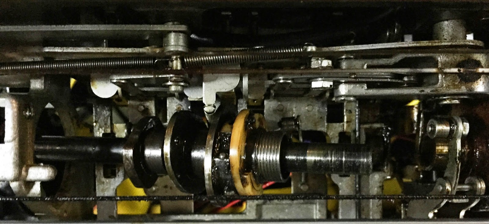
I lubricated more cams I found around the machine, meanwhile working each moving part to be sure it isn't sludged up. The read clutch spins with almost zero resistance, but there is still noticeable drag on the feed clutch. This may be normal, since it actuates so many cams that are pushing arms up and down, but I will keep at this for a while longer just to be sure it is as loose as necessary to ensure good reads.

NEW KEYPUNCH INTERFACE DEVELOPMENT

I had moved the keypunch around in order to get better accessibility to my 1442 for its restoration work. However, when I next tried to access the new interface box, the serial link is not working properly. At startup I get a line feed but no characters visible. Input from the terminal to the box is apparently not detected at all. Seemingly a hardware problem but essential to fix before I can debug further.

The path for the user serial signal is TTL RX and TX from the Arduino out to an RS232 adapter board, which generates and accepts valid voltages (not just the 5V of TTL). A straight cable runs out of the keypunch and up to a crossover adapter. That has a USB-Serial port adapter hooked in, with the USB link hooked to a PC running a terminal program. Lots of places something could have gone wrong.

I hooked the USB link to a different PC running a different terminal program, but saw the same results. That rules out some potential causes, but it could still be the USB cable, USB-Serial adapter, crossover adapter, straight cable, RS232 adapter in the box, wiring to the Arduino, or something I did in software that somehow disabled serial port stream output.

I was seeing the startup messages on the programming link (Serial) but nothing on the serial port for users (Serial1), so I just added a short message to display how my delimiter character prints. Suddenly, nothing coming out of the programming link either. Commenting the new message out restored the output from the programming link.

This means it is some very poor behavior of the Arduino environment, where the strings used for all my diagnostic messages are exhausting the dynamic memory space causing it to lock up. It would be very helpful if the darned thing were to emit some kind of alert when this happens. I now have to move all those fixed strings over to the code memory which has plenty of room - a tedious bit of code alteration but necessary.

With the strings moved over, the program was running correctly again. I took the box out and re-installed it into the keypunch to resume my testing. Now I was back in business. When I punched a card with a simple test message, I initially thought something was wrong because I saw extra holes in the card. However, it turned out to be correct behavior.

I implemented two ascii encodings - BCD, which is the original mapping developed by Stan Paddock for the first generation of the interface, and EBCDIC. I took every printable ASCII character, found the same printable character in EBCDIC and assigned it the Hollerith code. The mapping is pretty clean, but there are a few anomalies.

There are no equivalents to the characters [ and ] in EBCDIC, The ASCII character ^ is not in EBCDIC, but IBM has a logical not character on the keypunch which I substituted. EBCDIC has a cent sign but ASCII does not, at least not in the 7 bit standard character set. I reused the [ from ascii to generate the cent sign on the punched card. This allows me to produce all 64 standard keypunch characters on the 029 with ascii that matches (other than the cent and not characters which have substitutes of ^ and [ in ascii).

EBCDIC has hollerith codes for lower case letters, even though the keypunch keys only feature upper case ones. Since ASCII has both lower case and upper case letters, I implemented the two encodings. That is what happened with my test message; I had typed it in lower case on the terminal so it used the hollerith for that. The letter T in hollerith is a 0 and 3 hole, but the letter t is 0, 1 and 3 which is what was punched.

Card starts with 'test it ' in lower case, thus not usual keypunch code
Release is still not activating - will check my wiring again - and I am fine tuning the binary punching and automatic multipunching features. More testing but everything going very well and on track to wrap up the interface code in a few days.

SAC INTERFACE FOR ADDING PERIPHERALS TO THE 1130

I added more circuits to the second board, completing it by the end of the day. After some checking, I did find two mistakes that had to be rectified, with the erroneous parts removed but the replacements not yet added.

In addition, I removed the nine pairs of resistors on the first board which I had placed incorrectly. After I open the PCB holes on the boards for replacement resistors, I can solder them in to complete the first board.

This gives me 24 receivers and 24 drivers, out of a needed 41 and 36. Technically, a few of the lines could be just terminated coming in, because I really don't care about signals that tell me to run the usage meters to bill myself. Similarly, a few of the signals from me to the 1131 can be fixed in the off or on condition as appropriate, such as signaling that my usage meter is still running.

I will do a more accurate assessment of parts supply, since I am running low on two of the resistor types which I placed in correctly in almost a dozen spots so far. To be safe, I will order a few more of each now to be sure I can wrap up the final boards.

Saturday, November 1, 2014

Keypunch interface moving ahead, more SAC interface assembly and some mechanical work on the 1442 card reader/punch

1442 CARD READER/PUNCH RESTORATION

The National Museum of Computing in Milton Keynes, UK restored an 1130 system a while back. Based on the experiences they had with the 1442, I decided I too would be better off if I disassembled the card feed clutch to thoroughly clean out old lubricants. Its performance is critical to the timing of the card reading process - if it slows the card down then check conditions are forced, stopping the machine from reading the next card.

Feed clutch disassembled in center, read clutch upper left

Read clutch with belts and pulleys removed
In addition, I partly disassembled the read clutch and made sure it was moving freely. There are some cams driven by the feed clutch whose mechanisms and their pivots seem stiff. I will work on those too.
various cams on card feed shaft whose pivot arms and mechanisms need work
Part of the disassembly process had me use a pin punch to drive a pin out of the shaft;  the pin holds a pulley in place. After I had removed one pin and was carefully disassembling parts of that clutch, I heard a clunk. I couldn't find the punch anywhere in, on or under the machine. I have a feeling it shot somewhere inaccessible in the garage, but until I find it I won't be comfortably buttoning up the reader and running it.

Parts removed from 1442 in order to access the two clutches
I also heard a smaller clunk when I was hand rotating the read clutch shaft, with a small rod dropping down from somewhere. The rod has hemispherical ball ends. I am studying the parts catalog diagrams as this too much be understood before I can power up the reader. The good news is that I was able to get old gunk out of the clutches and good lubrication inside. The read clutch has a grease nipple in a location that was completely inaccessible while everything was together, but can now be used to force in new lube.

Grease nipple on card feed clutch now much more accessible
By disassembling things, I took on a set of adjustments after reassembly that wouldn't have had to be touched otherwise, but these clutches are so critical to the operation and timing of the reader that I thought it worth the cost.

Main card feed clutch latch and release

Card read clutch latch and release
I found a small roller that is frozen due to grease, part of the card feed mechanism. Most rollers I have already found and loosened up, but this one escaped my notice until now.

Little frozen roller above midpoint of picture


NEW KEYPUNCH INTERFACE DEVELOPMENT

After some investigation I did find out what was causing my flaky failure to recognize a registered card, as well as the reason that my initial testing of the ability to read cards was not giving me any valid hole values. My relay contacts were oxidized - slightly but enough to cause erratic results for the Card Lever relay which determines that a card is registered, while the Dup 3 relay that switches the sensing pins for reading during duplication were oxidized as open circuits.

I used some contact cleaner which claims to not damage anything nor to leave residue - a version of Deoxit without the lubricants or 'protectant's of the other Deoxit varieties. I got good values for both N/O and N/C contact closures on all poles, reinserted the relays and verified correct operation of the keypunch while disconnected from my box.

I then inserted my box and again verified that I could do everything with the keypunch, no odd behavior while I was connected. Finally, it was time to hook up a terminal and see how the interface works. I was able to command the unit and continue with the debugging of the interface.

I found an error in how I was error checking one command while in short verb mode, found that the release is not taking place at the end of a punch, suspect that two character encodings in my ascii table might be wrong, and am still not happy with how my binary mode logic converts four hex digits to a variable I later use for punching. I began looking at each and clearing them up.

I corrected the error checking bug, suspected that the release solenoid needs 20ms just like the space and row solenoids so adjusted it, and looked at the encoding issue. I discovered that the ascii to card code table which is a duplicate of the encoding from the original interface built for the 1401 project, is using a BCD character equivalent which prints differently on an 029; the 029 uses EBCDIC encoding of the hole patterns.

I decided that we need two standard tables for ascii translation, one to the BCD characters and one for the EBCDIC patterns matching ASCII printable characters as would be viewed on a terminal program emulating an ASCII device. ASCII itself has a separate encoding of card holes which we won't be implementing since this is not usual for the IBM computer environment and it could be handled by the USERTABLE option if needed.

I will build two tables BCDtable and EBCDICtable, adding a command for selecting which is invoked in MODE ASCII. The command is CODE BCD or CODE EBCDIC. The code is added and part of the testing underway. .

Testing continued, resolving the error checking bug and cleaning up the binary mode issue. Since the encoding is correct, but spurred a design enhancement, it is considered closed. The release is still not working and I found a couple of subtle flaws to clean up in the code. Looking at the release, I suspected the wiring but also the Release relay given the oxidation problem I had with the others.

Ran out of time tonight but making good progress on the keypunch interface. Hopefully the reading of the holes at the second station is not being blocked by oxidation on the sense pins, otherwise I will have to open up that station and clean up the contacts.

SAC INTERFACE FOR ADDING PERIPHERALS TO THE 1130

I  hooked up the TTL input and output leads to the first board. That one only needed the twisted pairs soldered onto the driver or receiver, as relevant for the direction of the signal, to make it operational.

I began a second board, but after three sets of circuits noticed I had made an assembly mistake on a number of the receiver circuits on the first board, swapping the position of a 1K and a 12K resistor. Sigh. I will have to clip them out, reopen the holes and then solder in replacements for the 9 bad circuits. I began by clipping and raising the faulty resistors.

Completed board but with misassembled resistors along bottom row clipped off and twisted up for replacement