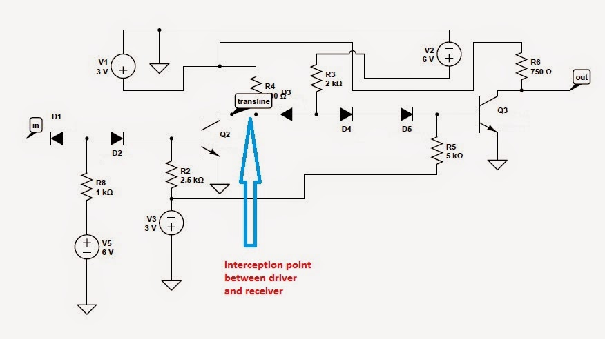
I spent some time during my cross country flights developing interface circuits that would take TTL logic levels and drive valid inputs to SLT logic, plus circuits to take SLT inputs and drive TTL logic outputs. These converters will sit between the Storage Access Channel circuitry in the 1130 and whatever logic I build to interface various devices to the 1130.
To do this, I started with the circuits used in the 1130 for sending the SAC signals out and for receiving inbound signals. One of the cards is defined in the online SLT designers documentation on bitsavers.org, but the receiver was not. By carefully studying all the various SLT and card schematic documentation, I was able to reconstruct the receiver card.
The transmission line driver and receiver for the SAC is the 30ns family AI without load resister feeding an AOI on the receiving end, the end of the line terminated by a 95 or 100 ohm pullup resistor to +3V.
The usual transmission receiver card has one input to an AOI (and-or-inverter, the basic logic gate of SLT) so it acts like a NOT gate but restores the logic signal. The driver is an and-inverter with just one input so it too functions as a NOT, but driving more current than a normal logic gate output, and with no pullup resistor on the collector of the inverter.
The receiver in the 1130 SAC uses two inputs in the AOI - acting as an AND gate, with one of the two inputs used to gate whether the incoming bit is passed on to the rest of the 1131. One such input is the 'write gate' that is set when a device is transferring data from a read into memory or during a cycle steal handling a read.
The usual receiver card has ten AOI circuits on board. The board in the 1130 SAC uses nine AOI - one AOI is used to receive the gating control signal, such as channel write gate, this signal then gates the other eight AOI which deliver the gated inbound bits.
Because of all the documentation, I am very confident that I have reconstructed the circuits on both sides. I was able to simulate them, verify the voltages, currents, transition points and other characteristics. This is necessary since my circuits will masquerade as a driver or a receiver, depending on whether a signal in outbound or inbound to the 1131.
 |
| Recreated 1130 SAC driver and receiver circuitry, showing point where my circuits replace left or right side |
The driver is even simpler - it is a transistor that will conduct when the intent is to send a logical 0, otherwise it lets the signal float. The 95 ohm terminator resistor on the far end will pull the line to 3V when we have a logical 1, and I will pull about 30ma of current through the transistor to drag the line down to near 0 volts for logical 0. I expect to have only a few millivolts at the far end, the result of wire resistance, transmission line mismatch and inherent resistance in the transistor - this will be well below the 300mv that is the cutoff for a valid logical 0 state.
I also developed all the rules for when I have to assert certain lines or latch in data, to implement the XIO instructions, interrupt handling and cycle stealing functions. It appears quite straightforward to produce a single device that connects to the SAC, although I want to design a more generalized interface that may have multiple devices connected simultaneously.
Over the coming couple of days I will work out the design approach for the generalized interface, allowing several devices to share the device. Whatever fpga board I use to implement this needs 76 I/Os for the SAC cable (36 output and 40 inbound signals), although I can disregard a few of them, e.g. CPU Meter In and Meter Out, since I don't care about running usage meters for billing purposes.
The board then needs additional IOs to attach all the intended devices. This will be a major design and sourcing factor. Most lower cost fpga boards have limited IO pins even if the fpga chip onboard itself has many hundreds of input/output pins - most are not connected externally.
No comments:
Post a Comment