Thursday, July 31, 2025

Removing and testing power supply box from 1132 line printer

ROLE OF POWER SUPPLY BOX

This box is connected to 115VAC, 208/230VAC, +6VDC, and 24VAC supplied over the power cable from the IBM 1130 system. It produces 48VDC to drive the solenoids such as the printer hammers and 20VAC to light the lamp for the encoder wheel. It provides a utility outlet typically used to connect an oscilloscope. It contains a usage meter with its control box that outputs 41VAC to turn the meter. 

The printer has a blower motor to cool the SLT electronics card cage, a carriage motor to advance the paper through the printer, and a main drive motor that spins the print wheels and character encoder wheel. Various switches and relays control power to the motors and parts of the power supply. 

In the 1130 system, a 24VAC circuit is routed to every frame in the system when the main console power switch is turned on. This voltage closes relays to power up the boxes. On the 1132, it activates relay K2 and contactor K1. K2 drains the voltage from the 48V power supply when the 1130 system power is off, preventing any printer solenoids from firing. K1 passes the incoming 208/230VAC from the CE power switch on the front panel of the 1132. 

When the 1130 system is plugged into the building power, the utility outlet receives power even though the 1130 system is powered down. When the 1130 main power switch is turned on, the fans in all the peripherals begin to run because DC power rails are energizing the SLT logic cards in all peripherals. It energizes relays and contactors such as K1 and K2 in the printer. On the 1132, the motor power switch on the printer front panel must be switched on to start the two motors and provide power to the 48VDC and 20VAC power supplies. 

REMOVAL OF POWER SUPPLY BOX

Rear of printer

Front of printer

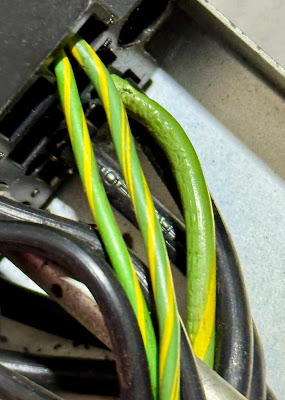
There are two terminal strips - one on the rear and one on the left side of the power supply box. The wires need to be disconnected from each of these, after taking a picture to record the connections. The box itself is held down by four bolts, two across the front and two cross the rear. 


The usage meter power/control box is separate, secured to the base by two screws. A medium size PCB sits on the right rear with three edge connectors around the periphery. It has the eight silicon controlled rectifiers (SCRs) and associated circuits to latch when a carriage control brush contacts the drum over which the carriage control tape passes. It also has some reed relays to handle the start and stop of carriage movement. 

Meter power/control box on left

On other peripherals the utility socket (US 115V wall socket) is on the power box, but it sits in a separate small box in the 1132. All the wiring up to the carriage motor and main power switch runs alongside the utility outlet box. 


Once I have all the wires disconnected, the box will be moved over to the bench to test it thoroughly. 

CONCERNED ABOUT THE CONDITION OF THE SCRS IN THE PRINTER

The circuit board with the eight SCRs (one for each carriage control channel used in the 1132) raised some worries. All the other components on the board look superficially okay except for the SCR parts themselves. The cans have quite a bit of rust on their surface. There is the possibility these may need to be replaced if contamination has entered the device itself or rusted the leads from the package to the PCB. 

ADDENDUM ABOUT CARRIAGE CONTROL TAPE

IBM line printers use a carriage control tape, a loop of heavy paper that is suspended between two drums and moves in concert with the paper carriage. Across the width of the tape sit eight metal brushes. If there is a hole punched in the tape in the column where a given brush is riding, the SCR will detect the connection. 

On the 1132 printer, there are brushes set up for columns 1, 2, 3, 4, 5, 6, 9 and 12. At any time, a programmer can test to see if there is a hole in the tape at the current line. The programmer can also request the carriage of the printer to skip forward, then stop the carriage when a particular column is detected. 

On most IBM printers, the programmer simply asks the printer to skip to a given channel; the printer carriage moves until it reaches a line where the tape has a hole in the chosen channel. On the 1132 this is something the programmer or system software must accomplish because the 1132 does not have enough logic in it to be able to skip and stop on a target column. 

By convention, column 1 is used to indicate the topmost line on a page of paper forms. The Forms Feed or similar button will skip the carriage until there is a hole in channel 1. Also, by convention channel 12 is used to indicate the last usable line on a paper form. The other channels tend to be used with special forms, allowing a program to jump down to a section of the form - for instance after printing a customer name and address, jump down to the list of items being ordered. 

The 1132 printer had the printer of an IBM 407 accounting machine inside its covers, wrapped in interface logic and new sheet metal to sell it as mid 1960s technology instead of the 1940s heritage of the 407. The 407 carriage control feature was part of the recycled components of a 407 that was used to build the 1132, thus the channels implemented were identical on both printers. Other printers such as the 1403 implemented more channels on the tape. 

Explanation from IBM 403 manual


Wednesday, July 30, 2025

Finished trace by trace and datasheet by datasheet examination; one issue arose that must be pondered

COMPLETED ALL THE DESK CHECKING

I very carefully examined all the data sheets and documented the pin assignments, footprints and logic rules for each chip used on the board. I then traced each signal on the PCB to ensure that it went exactly where it should and had the intended meaning. I submitted my final parts order and was preparing to send the design off to the PCB fab when I happened upon an unpleasant surprise. 

FOUND THAT STORAGE SELECT IS A PULSE NOT A STEADY SIGNAL

I happened to look at the ALD page that generates +Storage Select which I believed was steady state during a core access cycle. Instead, I saw that it is produced only during the T0, T4, X0 and X4 clock phases where it triggers a single shot to produce a pulse. After digging through many documents I finally found a chart showing the 100ns long pulses produced.

The logic page for the signal generation showed the circuit below.

The falling edge of any of those four clock pulses will trigger the single shot to generate a positive going 100 nanosecond pulse. A memory cycle on the 1130 is a sequence of eight clock steps T0 through T7. The first four are the read of the addressed word and the second four are the write-back (or update) of the word. Peripherals using cycle stealing (direct memory access in modern terminology) will instead do a memory cycle using clock steps X0 to X7 while the T clock idle. 

IMPLICATIONS OF THE PULSE

I combine +Storage Select with a sense signal showing +12V input is present, then combine that with +Storage Use to enable the MRAM chip. Further, that combination of 12V, +Storage Select and +Storage Use is combined with +Storage Read to enable the bidirectional pins on the MRAM to output the word contents. 

Because +Storage Select is only 100 ns, I will disable the chip before my read timer grabs the word contents from the bidirectional pins and outputs them to the CPU. Further, the chip will be disabled before my write timer gates the Storage Buffer Register (SBR) data bits to the memory chip bidirectional  pins and before I assert the signal to perform a write. 

RESOLUTION

While the CPU is actively running, executing instructions, the clock is advancing through the eight T or X clock steps. It is producing +Storage Read for 1.8 uS then +Storage Write for another 1.8 uS. It would be sufficient to use +Storage Use to enable the chip and +Storage Read and +Storage Write to trigger my timers. I could treat +Storage Select as a constant high signal. 

Now thinking about when the CPU clock is halted - a Wait instruction, the Stop button or other such conditions - The T and X clocks are both sitting idle. +Storage Write would still be active at the end of the prior memory cycle. The logic that generates +Storage Read and +Storage Write is shown below.

If any of T0, T1, T2, T3, X0, X1, X2 or X3 are active, the input on the left above will drive low which produces a logic high on +Storage Read and a logic low on +Storage Write. The clock stops at T7 and X7 when stopped/idle. Thus +Storage Write goes high at T4 of the prior memory access and stays that way until the clock starts again. 

My read timer triggers when +Storage Read goes high, which won't occur while the machine clock is stopped. My write timer triggers at the rising edge of +Storage Write, but the signal is steady high while we are stopped thus no triggering. 

Therefore, if I ignore +Storage Select and act as if it is logic high, the memory should still work properly. The detail of a memory access cycle below shows when events occur and how my design treats them.

  1. The machine is running or Start was pushed so that it is ready to advance from T7 and X7 at the end of the prior cycle. 
  2. If the +Storage Use is logic low, then we ignore any further signals for the cycle T0 to T7 (or X0-X7).  It is is logic high, we enable the MRAM chip with the E control signal.
  3. An address is placed on the Storage Address Register (SAR) and +Storage Use is logic high to request a memory access cycle.
  4. The machine moves to T0 or X0 clock step. +Storage Write goes low and +Storage Read goes high. 
  5. The read timer begins an 800 ns delay.
  6. The output enable signal G is set on the MRAM chip so that it will display the word contents on its bidirectional output pins
  7. The chip completes a read of the SAR address in about 35 ns, while we are still in T0 or X0, then leaves the data value on the bidirectional pins.
  8. The machine advances to clock step T1 or X1. The read timer is going to finish its 800 ns delay near the end of this clock step. The data from the addressed memory location remains on the bidirectional pins.
  9. The read timer starts an 80-90 ns control signal which causes any bit of the word that was a 1 to emit a logic low output on the -Sense Bit x line for the duration of the control signal. Other than when we have the control signal and a 1 bit on the bidirectional pin, the =Sense Bit x line remains logic high. 
  10. The CPU moves into clock step T2 or X2. The output on -Sense Bit x will finish early in this clock step. 
  11. The CPU moves into clock step T3 or X3. 
  12. The CPU moves into clock step T4 or X4. +Storage Read goes logic low, while +Storage Write goes logic high. The output enable signal G is deasserted and the bidirectional pins on the MRAM chip are in high impedance waiting to have data driven into them. The write control signal W is not asserted at this time.  
  13. The leading edge of +Storage Write triggers the write timer to produce an 800 ns delay. 
  14. The CPU moves into clock step T5 or X5. The write timer delay will go finish near the end of this clock step.
  15. The write timer produces an 80-90 ns control signal that is connected to the write control pin W of the MRAM chip and also to the enable pins of the buffer that gates the SBR data bits onto the MRAM bidirectional pins. 
  16. The MRAM chip performs a write in 35 nanoseconds using the data from the SBR at the address in the SAR. 
  17. The CPU moves into clock step T6 or X6. The write control signal from the write timer will end early in this clock step. The buffer stops driving the SBR data onto the MRAM bidirectional pins. 
  18. The CPU moves into clock step T7 or X7. 
  19. If the machine needs to stop, it stays in T7 or X7. It will advance to T0/X0 to start another memory cycle if it is not stopped. 

Thus my fix is pretty simple. I will adjust the schematic and PCB design then send it off to be fabricated. 

APPENDIX ON WHEN THE CPU IS STOPPED OR RUNNING

When in Run mode, the machine advances immediately to the next memory cycle. When the Start button is pressed, it advances to T0 for the next memory cycle. When a peripheral device requests a cycle steal to transfer data. the clock advances to X0. 

The CPU stops based on the rotary mode control, either after a clock step, a memory cycle or a complete instruction execution which entails multiple memory accesses. The Stop button and other conditions can also cause the CPU to stop, including execution of a Wait instruction. 

Tuesday, July 29, 2025

Extensive desk checking of PCB and final design for core memory replacement for 1130 system

PCB DESIGNED AND VERIFIED USING KICAD TOOLS

After about 22 hours of work I have a PCB layout that reflects my design for the replacement that will plug into the IBM 1130 and function as 8K of core memory. Assuming the final design is close to this, the bill of materials cost including the PCB fabrication plus all tax and shipping for parts is about $120. 


CHECKING CHIP BY CHIP FOR DATASHEET AND ACTUAL PCB CONNECTIONS

For each chip on the board, I will check the pins against the data sheet and the connections from those pins to other chips on the board. A particular kind of failure in projects like this comes from unseen shorts on the schematic in KiCAD that bridge wires that should not connect. The graphical editor sometimes sticks a dot over crossing wires, converting them into a connection. If I don't spot these subtle changes then the board reflects the faulty schematic and I will have wasted a round of PCB fabrication and soldering. 

I will check the package type for each chip as the pin numbering can vary. I want to be sure that the functional pin I wanted to connect is the one that has a trace on the board, including the other ends of the trace. 

SANITY CHECKING THE LOGIC

It is all too easy to send a signal that should be high but is inverted because of the driving circuitry. Also, complex chips that have many modes of operation depend on carefully understanding the datasheet and properly setting up the input pins to achieve the mode you intended. 

I want to model the flow of the external signals into the board and check that my thinking was sound. All logic conditions should work as I expected. No unexpected activations of signals should be possible. 

STUDIED VARIATION IF ONE OF THESE WOULD GO ON A DIFFERENT 1130 MODEL

The original 1130 models had 3.6 microsecond core memory, with one 4K or 8K memory module seated in gate B compartment C1 of the machine . Over time IBM expanded the product to larger configurations - up to 32K words by use of an expansion frame containing gates D and E to hold as many 8K modules as were needed to reach the capacity ordered. 

To support the larger memory, the machine has an Expanded Storage (ES) feature installed which re-uses gate B compartment C1 for additional logic cards to support the larger memory. With ES, all memory must reside in gates D and E since gate B compartment C1 is now unavailable. 

Machines without ES have three cables running from the rest of the CPU to the top of gate B compartment C1, placed in cable slots T1, T3 and T4. When ES is on the machine a fourth cable is also connected to T2. 

The machines with ES have three cables attached to gate B compartment C1 at slots A2, A3 and A4 which are connected to the installed core memory modules which would sit in gate D compartment A1, gate D compartment B1, gate E compartment A1 and gate E compartment B1. They hook directly to gate D compartment A1 and other cables daisy-chain to the remaining compartments based on the size of the total memory. 

IBM also changed the 1130 later in its life to offer a faster 2.2 microsecond core memory technology. This faster memory also requires the ES feature even for small configurations. A cable runs from the CPU to slot A5 of gate B compartment C1 to support the special needs of the faster memory. Therefore, any 2.2 uS machine has all its core memory in the expansion frame in gates D and E. 

My design would need to be modified to work with ES machines. Rather than plugging in the cables that normally hook to gate B compartment C1 connectors T1, T3 and T4, I would need to connect my board to gate B compartment C1 slots A2, A3 and A4. I would have to study how the signals are arranged on those cable connectors to determine any wiring changes on my board. 

In addition, the faster memory would require slightly different component values on my board to align with the 2.2 uS core behavior, but this is relatively trivial. 

I will look into this during the downtime once the PCB is ordered and I am waiting for the board to arrive. 

PARTS ARE ON ORDER FROM DIGIKEY ALREADY

I have ordered all the parts for the board and expect to have them all before the PCB comes back from the fab. Until I am satisfied with the desk checking I won't pull the trigger on the board so that starts the clock. 

Friday, July 25, 2025

High level design of replacement for 1130 core memory

INTERFACE BETWEEN 1130 AND CORE MEMORY

The interface is asynchronous, which eliminates the need to tie to the 1130 clock in any way. Based on the address being accessed, the appropriate core memory module is presented with +Storage Select. The 1130 logic asserts +Storage Use when it wants to do a storage cycle which is always a read followed by a write. 

The CPU raises +Storage Read during the first four 1130 clock cycles of each set of eight. The CPU raises +Storage Write during the second four 1130 clock cycles of the set. Since a clock cycle is 450 nanoseconds or 275 nanoseconds, depending on the speed of the core installed, this is either a 3.6 microsecond or 2.2 microsecond storage cycle. +Storage Read and +Storage Write are only approximately arranged relative to the 1130 clock. 

Core memory has destructive read, thus a storage cycle must write back the value that was in the word after it has been read. The core module addresses the particular word of memory during a cycle, sending current through the X and Y axis wires to flip the core towards the magnetic direction that represents a zero bit value. 

If the core had previously been magnetized in the opposite direction, which represents a one bit value, then the flip of the magnetic field induces a pulse in the sense/inhibit wire that runs through all the cores in a plane. It is the asynchronous arrival of this pulse that sets the Storage Buffer Register (SBR or B) to a 1 value. No pulse arriving leaves the B register set to a 0 value.

The B register now has the value that was destructively read out of the word. The cores are all magnetized in the zero bit value direction. The write cycle that immediately follows will write the value from B back into the cores. 

The write cycle sends current in the opposite direction down the X and Y wires, causing the core to flip to the magnetic direction thar represents a one bit value. Any bit in the B register that had a 0 value must have its core blocked from being magnetized during the write. This is done by sending a current through the sense/inhibit wire against the flow in the X and Y wires, thus inhibiting the core from flipping. No inhibit current means the core will flip to the one bit value direction. 

As long as the +Storage Select and +Storage Use signals are asserted, whatever address is presented on the address lines from the Storage Address Register (SAR) will select an X and Y wire to pick an individual word of memory. +Storage Read and +Storage Write alternate as long as the CPU is not stopped, driving first the read and then the write. 

When the +Storage Read signal goes high, the core memory sends the current through X and Y to reset the core to the zero bit value direction and any cores that were not already in that direction will produce a pulse on the sense/inhibit line. That pulse sets the B register to the value that was read from the word in core.

When the +Storage Write signal goes high, the core memory sends current through the X and Y to set cores to the one bit value direction. Any B register bit that is zero causes the sense/inhibit line to block that particular core from flipping, thus remaining in the zero bit value direction. 

Therefore my interface is the B register values as input, the sense pulse outputs, the SAR address as inputs, and the four control signals +Storage Select, +Storage Use, +Storage Read and +Storage Write

In addition to the sixteen data bits in a word, the 1130 employs two additional parity bits. Thus there are eighteen sense output signals. The B register provides 16 bit values as input. Some circuitry in the CPU calculates the proper parity and sends the P1 and P2 values as input to the storage. 

OVERVIEW OF MY CORE MEMORY SUBSTITION BOARD

The heart of this circuit is an Everspin MR0A16A Magnetoresistive Random Access Memory (MRAM). This chip has 64K words of 16 bits, is compatible with ordinary SRAM access patterns, and operates at 35ns. It can be read and written an infinite number of times without any degradation. It is non-volatile for at least 20 years when power is removed. 

The chip has bidirectional data pins, which are controlled by the output enable pin ~G so that the chip is driving an output when we want to read but when deasserted the chip can be driven with new data values to write into memory. The ~W pin requests a write of the data on the data pins into the addressed location of storage. The ~E chip enable pin is what we assert to cause a read or write (with the ~G and ~W pins appropriately sets. This chip supports independent access to the two bytes of the word, but we will keep the ~LB and ~UB pins asserted at all times to work in full 16 bit word mode.

Because the 1130 has two unidirectional data buses - B register and sense output - I will use a tristate buffer chip so that I only assert the B register and parity bit values when the chip is in write mode. In read mode we will route the data bits from the chip to a simple circuit that produces a pulse for any 1 value data bits about 800 nanoseconds after the +Storage Read goes high. I will also assert the B register/parity bit values to the chip about 800 nanoseconds after +Storage Write goes high. 

The circuit will have a voltage regulator to produce the 3.3V needed for the MRAM chip and related chips. The design of the MRAM chip will deactivate it when the power rail drops below 2.7V and won't activate the chip until the rail reaches at least 3.0V. 

I will feed the regulator from the 1130 system's +12VDC power supply. This supply is connected via a relay when the 1130 verifies that the three primary logic rails are stable at the proper voltage levels. If any of the power supplies sags, the machine is switched off, or the building power fails, this relay opens which immediately drops the +12V supply. This means we can't write anything unless the CPU logic is fully operational with good power and we will block writes well before the CPU logic rails drop. 

The 1130 puts its core memory in a separate card cage, either gate B compartment C1 or in gates D and E in the extension frame. It is connected to the rest of the system via three SLT connector cables that plug into the top of the card cage at positions T1, T3 and T4. I only need to provide SLT pins in the same arrangement as the backplane to allow those cables to be plugged into my circuit instead of the card cage. 

Mechanically, I will place the circuit board above the card cage but below the top grill of the card cage, right where the three SLT cables attach. The only other connection needed is a pair of wires to the +12V and ground lines. 

The MRAM chip needs to be shielded from stray magnetic fields that can disturb the stored values. I will put a metal faraday cage around the chip on the PCB to provide this protection. I believe that with surface mount parts, I can make a board that fits in this space, however if not I will work out an alternative. 

Thursday, July 24, 2025

More parity error instances - new fault in the core memory stack

PREPARED TO RUN THE DIAGNOSTIC BUT IT HALTED WITH PARITY ERRORS

I used the memory loader to place the 309 diagnostic into memory and then started it running at location 249 so that I could hit interrupt request to cause the diagnostic to begin running. I found the machine stopped with a parity error. 


The data from memory (Storage Buffer Register) had four bits turned on in the left halfword, which would require the P1 parity bit to be turned on to achieve odd parity. Since it wasn't on, the system stopped with a Parity check. The right halfword has one bit on and the P2 bit is correctly at 0 to result in odd parity for that side. 

Some parts of the display are difficult to read, an artifact of the scan rate of my phone camera and the display lamp operation. The Instruction Address Register is 0389 and the Storage Address Register is 0388. This is fetching an instruction (I1 instruction phase) which appears to have been a BSC I instruction with an offset of 0010. We don't know the second word of the instruction because we stopped on the fetch of the first instruction word (I1). 

I tried resetting the machine and running, but got three more Parity Check stops after each attempt. 


There is not enough visible on the first of the three stops above other than it failed while reading the operand of an instruction (E1 instruction phase) from location 0201 where it appears it received a word of 0000 but the two parity bits P1 and P2 were not set. I suspect this was an artifact of stopping and resetting the system after the prior Parity Stop.

The second of the three stops above has IAR of 028D meaning we are executing the instruction from 028B and 028C. The instruction was interpreted as a 68xx which is a register update instruction, picking up a value from 0015 which has a parity error in the left half. 

The last of the three stops above has IAR of 0005 with an SAR of 0005 and the SBR left halfword with three bits on does not have the requisite P1 bit set. 

A common feature of three of the four is bit 3 being set with a parity error in that halfword. I checked this by doing a Storage Load function on the console setting 0000 to all locations in memory. When I ran the Storage Display function we stopped with bit 3 on and a parity error. 

BIT 3 IS WRITTEN AS A 1 EVEN WHEN 0 IS INTENDED - INHIBIT FAILURE

I stuck a voltmeter on the inhibit input to memory for bit 3, turning the machine to Load mode where the input to memory will be the console entry switches on the front of the machine. As I flipped switch 3 up and down, the voltage flipped between 3V and nearly ground, indicative of proper input from the 1130 to the memory gate.

This is almost certainly an inhibit failure for bit 3. When the memory does a write cycle, the X and Y lines try to flip the addressed core to the 1 direction. If a reverse current flows through the inhibit/sense wires, the core will not flip to 1; if no inhibit current, then we set it to 1. Regardless of the logic level that is input to the inhibit, the core flips. 

l tried various addresses and confirmed that bit 3 will ALWAYS be written to 1 for addresses from 0 to 4097, but the bit works properly for addresses in the second 4K of memory. This localizes the error to the low 4K circuitry. 

CHECKING RESISTANCES ON THE STACK MAY SHOW OPEN GROUND CONNECTION

I did a quick ohmmeter check on the pins going to the sense/inhibit wires for bit 3 in the low 4K and saw indications that the ground connection might be an open circuit. To make a more definitive test I have to pull the sense/inhibit driver cards before I test the wire resistance. However, this is a type of failure we have seen before. 

MULTIPLE FAILURES HAVE OCCURRED ON THE SAME PCB BOARD IN THE STACK

The core memory stack that is mounted in the center of the memory logic gate has printed circuit boards at the bottom and top of the sandwich, as well as eighteen core memory planes in the middle. The top PCB holds the steering diodes that allow a reasonable number of drivers to connect to any of 4098 cores in a plane for a 4K segment. The bottom PCB routes signals from the edges of the PCB to pins arrayed across the bottom area. 

Wires from the core planes run down to be soldered onto the edge of the bottom PCB. These signals follow traces to pins that stick down out of the bottom PCB. These pins fit through holes drilled in the glass backplane. On the rear of the backplane, connectors bridge the pins from the memory stack to pins attached to the backplane. This is how circuitry on the backplane is connected to the core stack, with logic cards arranged around the sides of the backplane. 

The trace is not visible from the bottom of the core stack, as they sit on the surface under a core plane. Thus I have no way to look inside nor to make repairs. Trying to take the sandwich of layers apart would involve unwelding many connections to all those core planes. 

I have run jumper wires to bridge open circuits that were discovered when other parity problems arose in the past during the restoration of this system. There is no sign of a crack on the PCB and no commonality in the areas where the pins for the failed circuits are mounted. I suspect some kind of erosion or contamination, perhaps mouse urine from the extensive infestation this machine suffered in past decades. 

MY FEAR IS THAT THE SYSTEM WILL EXHIBIT ADDITIONAL FAILURES OVER TIME

If this is yet another failed connection, I might be able to jumper it but the reality is that if we have encounted progressive failures to date, it is likely those would continue. There are a total of 108 connections for sense/inhibit lines across the 8K core stack. 

Until I finish careful debugging of this new parity issue, I can't be certain that it is a new break in the lower PCB of the stack. If it is, that will be disturbing. 

INVESTIGATING AN ALTERNATE 8K WORD MEMORY FOR THE SYSTEM

The interface between the rest of the IBM 1130 and the core memory gate is pretty simple. The memory, with a read-then-write that takes place over a glacial 3.6 microseconds, will be very easy to replace with a substitute. 

It should be non-volatile, just as core memory is, thus I am investigating devices such as MRAM chips that have plenty of speed, capacity, infinite lifetime of reads/writes and decades long non-volatility. 

More restoration work on 2501 Card Reader - buttons, lights, cable repair, short circuit check

CHECKING DC VOLTAGE RAILS FOR POSSIBLE SHORT CIRCUITS

The IBM 1130 system supplies all the power to the 2501 Card Reader through a power cable between the two machines. It carries 230VAC, 115VAC, 7.25VAC, frame ground, DC ground, 6VDC, 3VDC, -3VDC in that one cable, with a multipin connector on each end. All the logic cards inside the 2501 receive the power rails (+6, +3 and -3) over this cable. 

Prior to cabling the machines together and turning on power, I tested the DC power inputs to check for any short circuits. If those existed they would generally be the result of a filtering capacitor failure. The SLT logic cards contain tantalum filter capacitors on the rails. While I very rarely see the capacitors fail in an SLT machine, there have been a couple of cases where they were found to be shorted. 

These shorted capacitors were filtering a 48V rail which is far too close to the nominal rating of the capacitor for safety. Solenoids in the console printer, paper tape devices, console keyboard and a few other devices operate 48V. I have never seen an IBM tantalum from this generation of computers fail other than with 48V solenoid circuits. 

The three main DC rails had tens of kilohms immediate resistance which quickly climbed to hundreds of kilohms, essentially due to charging up all those filter capacitors. This cleared the 2501 to be powered from the 1130. 

PUSHBUTTONS AND MICROSWITCHES

The 2501 card reader has three operator pushbuttons on the front panel - START, NPRO and STOP - plus a number of microswitches throughout the machine for sensing various conditions. Switches detect when the input card hopper is empty and when the output stacker is full. Switches detect when the cover of the reader is opened and when a service bypass switch is thrown. Contacts on the motor relay indicate when the motor is not powered (i.e. stopped). 

I checked the continuity and appropriate resistance of the buttons and microswitches. IBM placed a 620 ohm resistor in series with the pushbuttons, which makes the machine relatively insensitive to oxidation resistance on contacts. Most of the microswitches make or break contacts, but we have one toggle switch (service bypass) and magnetic reed switch (cover closed). 

All of them looked fine except for the hopper empty switch. A spring loaded projection rises through the bottom of the input hopper. Any punched cards placed in the hopper will push that projection down, activating the microswitch. Neither the normally closed nor the normally open side of the switch had continuity. 

RESTORING OPERATION TO THE HOPPER MICROSWITCH

I unmounted the microswitch and took it to the workbench where I partially disassembled it. Using Deoxit, I was able to restore good low resistance operation of the switch. I reinstalled this on the card reader and verified from the logic gate that the switch contacts were opening and closing as intended. 

MANUFACTURING DEFECT IN POWER CABLE CONNECTOR REPAIRED

When I examined the end of the power cable connector, I saw that one pin was pushed down into the connector so that it would not make good electrical contact when the connector was hooked to the 1130 system. This pin was the AC frame ground pin. 


The connector type has pins that are pushed through the connector body from the back until they snap into position, locking them fully up. This particular pin had not snapped into place, something that most likely occurred during manufacturing and was never caught. The machine would operate properly but the frame wasn't bonded to the 1130 frame and the ground pin to the building power supply; this was a safety issue that would lurk undetected for years of operation. 

When I opened the connector, I could see that the frame ground wire was taut, not allowing the pin to be pushed far enough in to snap into a locked position. I realized that I had to provide a bit of looseness to that wire if I hoped to repair the connector and make the reader safe for users. 

Inside the housing

Problem pin not pushed in far enough

Wire too taut (diagonal from lower left)

After pulling everything apart, I moved the rubber sleeve down on the cable and tightened it in place so that the wires were a bit further into the connector housing. This gave me the needed additional millimeters of wire to push the pin fully into the housing and snap it into position. 

Pin now locked in place

Visible slack on wire

After reassembly the power connector will make full contact on all power pins including the AC frame ground. 

CHECKING LAMP CIRCUITS - WITHOUT POWER

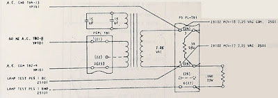
The basic circuit for the indicator lamps has a custom IBM SCR (Silicon Controlled Rectifier) that has the usual three terminals plus a lamp test terminal with an internal decoupling resistor. Power for lighting the lamps is produced inside the IBM 1130 with a very sizable transformer producing 7.25VAC to drive all the lamps on the 1130 and all its attached peripherals. 

Circuits in the 2501

One side of the 7.25VAC power supply output is connected to the system's AC ground and to the DC ground terminal strip. This side of the power supply is hooked to the G pin of the IBM SCR. The other side of the power supply is hooked to all the lamps. Each lamp, besides connecting to one side of the 7.25VAC supply, is also connected to the A pin of the SCR. 

Power supply in 1130

Lamp Test switch in 1130

The S pin of the SCR is the gate of the device - a positive voltage between S and the G pin will cause the SCR to latch on through one half-cycle of the AC supply until the AC voltage reaches the 0 point at the end of the half cycle. Thus, the lamp is driven by the positive half cycle of the AC supply as long as the signal is positive, but is off when the S input is at or near ground. 

The Lamp Test switch on the main 1130 frame connects the 7.25VAC to the T input of all the SCRs in parallel - the side of the AC that is opposite the side connected to the G terminal. This drives the SCR through all the positive half-cycles while the Lamp Test switch remains pressed; the connected lamps light up to allow detection of any burned out bulbs. 

I verified that the SCRs had appropriate diode action across all the relevant pins. What remains is to power up the circuits with a bench 7.25VAC supply and check that the bulbs light when the signal input S is high, or when 7.25VAC is applied to the T input, but not otherwise. 

Since the connection of one side of the 7.25VAC power supply output to AC and DC ground is done inside the 1130 frame, I will need to wire the bench supply appropriately to all the input pins on the connector. I can then switch on the 7.25VAC manually to the T pins and switch +3VDC to the S pins to complete my testing. This will take place in my next visit to the workshop. 

Wednesday, July 23, 2025

Reinstalled the power box inside the 2501 card reader

INSTALLED BACK IN BASE OF THE READER

The power box fits on top and bottom rails inside the card reader enclosure, on the right side. I installed it and replaced the cover. 


The power box is connected to several other parts of the card reader. I describe a bit about the type of connection and how it is made in the sections below. 

AC CONNECTED TO UTILITY OUTLET AND POWER BOX

The 2501 card reader is connected via two thick cables to the IBM 1130 system. One of the cables carries data signals while the other brings power to the 2501. The power cable is split out inside the 2501 enclosure into an AC and a DC connector. The DC connector brings the SLT logic power rails from the main system - +6, +3 and -3V. The AC connector brings 230VAC, 115VAC, and 7.5VAC for the lamps on the control panel. 

The AC connections for the lamps are routed separately, but the other AC voltages are connected through a bundle of wires clamped at the bottom of the power box. The 115VAC is connected only to the utility outlet - that outlet has power even when the 1130 system is powered down, typically used for oscilloscopes or other repair related equipment. The 230V is used to drive the motor and to produce some additional AC and DC voltages used in the card reader. 

USAGE METER CONNECTED

A usage meter records the time that the 2501 is active; IBM in the past had rental plans where users were charged based on usage of the computing systems. A power supply on the outside of the main power box produces the 41VAC that turns the usage meter and contains the control circuitry to start and stop the meter. A pair of wires run from the usage meter on the top of the card reader down into the usage meter power box. Another pair of wires runs from the usage meter power box over to the SLT card cage, to detect when the reader is active or idle.

LAMP POWER FOR READING AND CARD DETECTION

A pair of lamps are used inside the 2501. One of them shines onto a photocell that detects when a card has entered the pre-read station and is available for a read or feed operation. The other shines through fiber optic cables to the 12 card row positions to illuminate 12 photocells underneath the card if there is a hold punched in the card at the current column. 

Two pairs of wires are connected to terminal strips on the outside of the power box, one each for the two lamps. 

MOTOR POWER

The main motor that drives cards through the machine is connected via a cable that runs from the top of the reader where the motor is attached down to the power box. The power box will turn on the motor when a read, feed or non-process run out (clearing cards from the machine) is requested and keep it running for 15 seconds. If a series of reads take place the motor thus stays running continuously but is shut down when idle for 15 seconds or more. 

SIGNALS AND CONTROLS BETWEEN LOGIC GATE AND POWER BOX

The power box produces 24V to activate various solenoids that feed cards inside the reader; the power is connected from the power box to the logic gate which in turn sends the power to the solenoids. A number of control signals are connected between the logic gate and the power box. For instance, the signal to turn on the motor is sent to the power box and the timer indicating that 15 seconds has not elapsed is sent back to the logic gate. 

NEXT STEPS - TEST THE LAMPS, PUSHBUTTONS, MOTOR AND SOLENOIDS

Before I connect the 2501 to the 1130 I will check out the indicator lamp circuits. These run on 7.5VAC and will illuminate when +3V is present on the control wire or be dark when the control wire is at ground. I can isolate these and test them. The circuits use an SCR to drive incandescent bulbs. Generally the bulbs are the most likely to have failed.

I will also verify that the various pushbuttons have good connectivity and operate properly. They may need to have oxidation cleaned out. 

Once all of the above is complete, I am ready to apply power to the 2501 from the IBM 1130 and begin some testing. The NPRO button triggers a non-process run-out, meaning it feeds cards that may be inside the reader to flush them out to the stacker but does not feed cards in from the hopper. The START button will trigger a feed cycle, moving a card from the hopper into the reader. Both of those allow me to verify that the motor starts, stays on for 15 seconds without further activity, and that the two feeding solenoids are activating. 


Tuesday, July 22, 2025

Discrepancy in logic diagrams and theory of operations documentation

FOCUSING ON TIMING OF SEEK CONTROL SIGNALS

The disk drive receives three signals from the 1130 disk controller logic:

  • Access Drive (Access Go)
  • Access 10-20 Mil Step
  • Access Direction
The drive sends back a signal Access Ready that indicates when it can accept a seek request and shows the progress of the seek (crudely). Roughly, the Access Ready signal is true when the drive becomes ready and will switch to false about 5 ms after the seek begins, returning to true in a further 10 ms. 

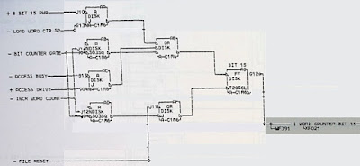
The disk drive logic manuals describe Access Go as a brief pulse. Since it is inverted logic, -Access Go drops from high to low briefly to request a seek. The wiring diagram for the 1130 shows that -Access Go on the drive is directly connected to -Access Drive in the 1130 controller logic. 

The problem with the above is that the logic producing -Access Drive does not generate a pulse. It asserts the signal by making -Access Go low when the +Access Busy signal goes high at the same time that +Access Ready is high and -Full Word Count is high. 

The +Access Busy flipflop is switched on during an XIO Control (seek) instruction at time T6 as long as the count of cylinders to be traversed is not zero. The condition -Full Word Count is high when the cylinder count is non-zero, reaching zero when the final movement of the arm exhausts the requested number of cylinders to move. 

+Access Busy stays on for the entire length of a seek request, while +Access Ready turns on and off with each 1 or 2 cylinder step taken by the disk drive. That is because the drive only knows how to move 1 cylinder (10 mils) or 2 cylinders (20 mils), forward or in reverse. The +Access Go is sent to trigger each step, with the cylinder count decrementing until we complete the transfer such that -Full Word Count goes low. 

As long as +Access Busy is on (not done with the seek command) and -Full Word Count is high, we will repeatedly trigger the -Access Drive signal, each time it make the disk drive take another step. This happens because +Access Ready is high. When +Access Ready goes low in the midst of the step, it turns off the -Access Drive signal. 


The disk drive is causing the alternation of the -Access Drive signal is the feedback signal from the disk drive, +Access Ready. When +Access Ready is high, we retrigger the next step until the full word count (cylinder count) is reached. When +Access Ready is low, we reset the -Access Drive signal. 

The timing of +Access Ready from the disk drive has it go low about 5 milliseconds after the drive accepts a step request (i.e. -Access Go becomes low). It remains low for another 10 milliseconds then returns to high. The time to go low varies depending on whether this is a 10 mil (1 cylinder) or 20 mil (2 cylinder) step. 

If we issue an XIO Control (seek) for 7 cylinders total, the word count is set to 7 initially. The controller logic sees an odd count thus it initially requests a 10 mil step. The word count is reduced by 1 and the step size now reverts to 20 mil for all further steps. Thus the word count first drops to 6, then is decremented by 2 on each step until the count gets to zero where our -Access Go is no longer issued. An even cylinder count begins and continues with 20 mil step sizes. 

The timing chart for the disk drive has a brief pulse for -Access Go while we see from the controller logic side that instead it does low for about 5ms and then returns to high. 


The state of the +Access Direction and +Access 10/20 Mil Step signals is shown as changing simultaneously with the supposed -Access Go pulse. The notion of simultaneous is a bit slippery when dealing with signals in an 1130, where everything is a bit asynchronous and not based on clocked flipflops like modern designs. 

The +Access Direction signal is set or reset during the execution of an XIO Control based on bit 13 of word 2 of the Input Output Control Command (IOCC). That means at clock step T6 of the XIO step E1 the flipflop below is set and it is only changed at the next XIO Control, thus it remains constant through the course of an entire seek operation. 


The +Access 10-20 Mil Step signal is generated from the word count register - it is the same as the low bit (bit 15) of the register. During the XIO Control step E2, at clock time T4, the cylinder count is loaded into the word count register. 

The bits are inverted - thus a count of two (0000 0000 0000 0010) would load as (1111 1111 1111 1101). It looks at the B register (Storage Buffer Register) and when the bit is 0, the word count register bit is turned on. 

The very first time that -Access Go turns off during a seek, bit 15 is forced on. Thus, if the low order bit of the seek request - B bit 15 - was 1, for an odd count, the word count register starts off with its bit 15 set to 0 but after the first step it is forced to 1 and stays that way. Word count register bit 15 is interpreted as +Access 10-20 Mil Step, when it is 0, the step is 10 mil and after it is forced to 1 the step size is 20 mil. 

Thus, +Access 10-20 Mil Step will change when -Access Go is turned off, which is due to +Access Ready from the disk drive becoming false. It initially changes when the XIO Control command is being processed and then changes either once after the first step or stays constant for the duration of the seek command. 

HOW THIS MAY IMPACT MY FPGA LOGIC IN THE V2315CF

This compares poorly to the timing shown in the disk drive documentation, which implies that the direction and step size signals change simultaneously with pulses on -Access Go. My logic was based on the documentation for the disk, but I can see some weaknesses based on what I discovered and documented above. 

+Access Direction should be captured before the -Access Go signal goes low to start the timing of a step. I shouldn't see it change until the next XIO Control is issued. +Access 10-20 Mil Step will be set before the first -Access Go step and may change at the end of the first such step, before the next step is requested. I should capture the change while -Access Go is high and not change it until we finish a step of the arm. 

My earlier logic for the state machine looked for edges on the +Access Ready and -Access Go signals, but the logic of the controller moves grossly based on the ~5ms and ~15ms timing of +Access Ready. I don't know whether it is possible to get glitches on those signals, as their timing should move on a relatively glacial scale. I may slightly debounce them in addition to passing them through a metastability chain of flipflops. 

One final consequence of the way the logic functions is that when +Access Ready returns to high, the controller logic is going to be asserting -Access Go fairly quickly and I need to be ready to trigger off it. I am fairly certain that I already did this properly, but will double check. 


Running IBM disk diagnostic 309 against the Virtual 2315 Cartridge Facility - part 11

 MODIFYING DIAGNOSTIC 309

I first attempted to verify the values being loaded into core memory against the listing of the 2310B Function Test (diag 309), but found differences from the version I had documented. I then decided I had to put in a wait at an appropriate point in order to verify that the seek command is being properly set up. 

COLLECTING DATA ON FAILURES

Fired up the diagnostic program with it set to wait just before it attempts the seek to cylinder 199. This has been failing, stopping at cylinder 196 instead of 199. What I observed from the Input Output Control Command (IOCC), a doubleword pointed to by the XIO instruction, is that the count for the seek was set to 199 as it should have been. 

WHAT THIS RESULT SUGGESTS

Since the IOCC was correct but the drive didn't move all the way to the correct location, this hints at some interaction with the running code or the interrupt handler of the diagnostic, considering that a hand coded XIO seek to 199 performs correctly when executed in single instruction mode. 

DID MORE MANUALLY CODED SEEKS AND SEEING SOME ANOMALOUS BEHAVIOR

I did seeks to intermediate cylinder locations - 160, 180, 190, 200, and 197. In each case, I first did the seek forward from the home location (cylinder 0) and then did a reverse of the same distance. Mostly these worked properly, but I then hit some odd cases.

In one case, although I had set up a reverse seek to head all the way back to the home cylinder, the arm instead moved forward and then pushed on the stop at cylinder 202. In another case, when I moved all the way forward to be at the final cylinder the system no longer responded to seek commands in spite of the Seek lamp on the Virtual 2315 Cartridge Facility (V2315CF) box. 

WILL RE-EXAMINE AND RECODE THE SEEK LOGIC IN V2315CF

I now suspect malfunctions in the state machine in the seek to cylinder module of the FPGA logic. The non-responsive condition must be a stall in the state machine. Also, if it stalls in an intermediate state it might leave the direction signal in a previous state, causing the anomaly where the arm moved forward instead of in reverse. 

I will also think more deeply about the corner cases - making sure my logic will track properly. 
  • when an XIO Seek is issued to back up but the arm is already at the home cylinder
  • when moving forward from a high location more than the remaining cylinders
  • when trying to move forward from cylinder 202
In real mode (the drive actually moves the arm as well as the virtual arm inside the V2315CF), the seek to cylinder logic is needed to shadow the position of the real drive arm, allowing us to know the current cylinder. This is necessary to feed or update the proper data from the virtual cartridge image, that intended for the cylinder.  

The real drive is the one responding with signals such as access ready to the signals such as access go from the 1130 disk controller logic. We sit in the middle and count the movements to maintain a cylinder number that should be synchronized with the real drive arm. 

Replaced circuit breaker on IBM 1130 +6V power regulator

WEAKENED CB TRIPPING INCORRECTLY

As I had determined, with the machine drawing less than 9A from the +6V power regulator, the CB will trip off when power is turned on if it was warm. I power up the 1130, run for a while, then when I want to turn off power for a short time before turning it back on, the breaker will trip off. 

+6V power regulator

FIRST TRY AT ORDERING REPLACEMENT CB FOILED BY VENDOR ERROR

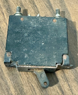
I bought a 25A CB that is close enough to the one included in the regulator. When the shipment from Amazon arrived, I discovered a problem. The plastic package listed the product as a 25A breaker, but then breaker inside was a 10A unit. I returned it to Amazon and waited again for the correct breaker to arrive.

Replacement breaker

MECHANICAL FIT IN THE REGULATOR

The failing circuit breaker provides three additional terminals which are used to indicate whether the breaker is turned on or off. The IBM 1130 does not make use of these, thus the replacement breaker didn't need that. I removed the wires for the indicator from the breaker and the regulator terminal block at the other end. 

The replacement breaker is nearly the same size, but differs in its width, thus the two mounting holes are too close together to have both attached with screws. 

Test fit

I was able to mount the new breaker  in the same location, using one screw. It seems well enough anchored. I wired it up and replaced the regulator in the 1130 system. 

Ready to re-install

Failing breaker

TESTING ABILITY TO CYCLE 1130 POWER WHEN IT HAS RUN FOR A WHILE

I brought up the system and did some work on it, letting the regulator warm up. I then flipped off machine power, waited 60 seconds, and turned the system back on. The power cycle worked exactly as it should. Annoyance resolved. It was occurring often enough that it would have been intolerable at its home when attempting to show off the working 1130 system. 


Wednesday, July 16, 2025

Running IBM disk diagnostic 309 against the Virtual 2315 Cartridge Facility - part 9

ANNOYANCE - THE +6V REGULATOR TRIPS ITS CIRCUIT BREAKER WHEN WARM

There have been lingering problems where the circuit breaker on the voltage regulator module for the +6V supply will trip off as if it had overcurrent. This often happens when the machine has been running for a while, is shut off and then turned back on within a couple of minutes. 

I hooked wires to the load resistor inside the regulator which senses the full current flowing out of the regulator. It is nominally 0.072 ohms and the voltage drop across it should tell me the current being drawn out of the regulator. If it is 1.728V or less when the 1130 system is not drawing more than the 24A capacity of the regulator - that would indicate that the circuit breaker itself is weakened and needs replacement. If the sensed voltage is higher then I have to find the components drawing excess power and repair them. 

My voltmeter showed a consistent .607V drop across the resistor. I had verified that the resistor was just over 0.07 ohms using a sensitive ohmmeter, thus Ohms Law indicates the current being consumed by the 1130 system was fairly steady at just under 8.5 amperes. 

This tells me that the circuit breaker is very likely to be faulty. The regulator would need to be consuming more than 200W for the CB to be near its limit yet the system draw of 8.5A regulated to 6V is only a quarter of that. The regulator can't be that inefficient. The unregulated input power is a bit over 8V thus it should be in the 70% or higher efficiency range. 

I ordered a replacement - not an exact copy but should be able to fit it into the regulator in place of the original breaker. 

HALTED DIAGNOSTIC ON FIRST ERROR - DRIVE IS INDEED SEEKING TO 196

The diagnostic program begins by seeking backwards to the home cylinder, which is indicated by a microswitch on the drive that signals when the arm is at cylinder 0. It then issues a seek of xC7 - 199 cylinders forward. The seek ends with the arm stopped at cylinder 196 which is consistent with the data my V2315CF returns when a sector is read after the seek. This means we either have a controller unit logic defect in the 1130 or a diagnostic program error. 

DID A SINGLE XIO SEEK FROM HOME FOR 199 CYLINDERS

I then hand coded an XIO to seek 199 cylinders from the starting (home) position. In this case, the arm correctly stopped at 199, not 196. I have to validate that the diagnostic program is issuing the correct XIO seek command. I will load the program into core and then stick in a wait instruction right after it has prepared the IOCC for the seek and before the actual XIO is issued. 

I can examine what was generated and then let the program continue to issue the seek and evaluate the outcome. This should permit me to point the finger of blame at diagnostic or controller logic. 

Monday, July 14, 2025

Running IBM disk diagnostic 309 against the Virtual 2315 Cartridge Facility - part 8

TESTING IN REAL MODE

With the V2315CF set to real mode, the 13SD disk drive inside the IBM 1130 runs and participates in the disk activity along with the V2315CF. With a virtual cartridge loaded into the V2315CF and any old physical 2315 cartridge loaded into the 13SD, flip the motor power switch on to spin up the drive. 

Once the disk drive finished its 90 second purge of dust from within the spinning drive, the File Ready lamp on the 1130 main console lit up as well as the RDY light on the V2315CF box. The 13SD drive believes it has lowered the heads onto the surface of the spinning platter, but they remain safely above. This made the disk ready to be accessed by the diagnostic or any other program on the 1130.

INITIAL FAILURE TO RUN TRACKED DOWN TO A BROKEN WIRE

When I began to test, the 1130 never indicated that the drive became ready. The FILE READY lamp should have illuminated, as well as the RDY light on the V2315CF box. I did hear the solenoid on the disk drive click on to load the heads down, which should have sent a signal -File Ready from the drive to the V2315CF and onward from there to the 1130. 

A quick check with a continuity tester identified the wire which carries that signal was broken in the cable. After a bit of work, the connection was restored and the drive ready state would recognized by the 1130. 

TESTING RESTARTED

The diagnostic moves the disk arm around first to verify the behavior of the Home (cylinder 0) detection and correct arm movement. Once it backed up to the home cylinder, it executed a seek to cylinder 199 but based on the data read back from the V2315CF, we believed we were at 196. A second attempt to move to 100, by seeking 3 cylinders forward, retrieved data from cylinder 197, but after that the system did sync up at 199. 

Test routine 2 began, which would perform patterns of seeks such as two cylinders forward, one cylinder back, each time reading a sector to verify the proper location was achieved. At some point during this test, the diagnostic issued a diagnostic complaining that after it issued an XIO instruction, the disk drive device status did not indicate a busy condition, just a not ready status. 

Shortly thereafter the diagnostic reported that a completion interrupt never arrived. This caused the diagnostic to terminate. My analysis of this is that the controller logic set the drive to not ready status, as if it had been switched off manually. The next XIO attempt would produce exactly the symptoms detected by the diagnostic. 

I don't know why the disk went off line like it did, but I will work out a test plan to track down the cause. Further, I have an easy way to point the blame for the initial seek failures, by setting the diagnostic to halt on the first error. Thus when it attempts to seek to cylinder 199 and receives data from cylinder 196, I can compare the disk arm in the physical 13SD drive to both of the reported locations. 

If the disk is at 199, then the failure is in my V2315CF. If the drive is at 196, then the failure is in the IBM 1130 disk controller logic or in the drive itself. 

Monday, July 7, 2025

Very sporadic parity errors - need to capture evidence to find and fix

TYPEWRITER DIAGNOSTIC RANDOM PARITY ERROR WITH BIT 10 FALSELY DETECTED

I snapped a picture of a parity error stop that popped up randomly while the typewriter diagnostic was running. The 1130 was fetching the next instruction to execute from location x0258, which you can see from the Storage Address Register (SAR) in row 2. The process of fetching the instruction causes the Instruction Address Register (IAR) in row 1 to be bumped up by 1, which is why it shows x0259. 

The data read from memory is in the third row, the Storage Buffer Register (SBR), with xC220 showing. Looking at the listing for the diagnostic monitor running the typewriter diagnostic, at location x0258 is a LD 2,0 instruction - load from the address in index register 2 plus a displacement of 0. This would be xC200 but we have bit 10 turned on incorrectly. 

Each half of the memory word has its own parity bit which is set so that the total number of 1 bits in the half of a word plus that parity bit must be an odd number (odd parity). The left half has bits 0, 1 and 6 turned on, an odd number, so parity bit P1 is off (middle section of the display panel). The right side shows bit 10 on (the error) which would be an odd number of 1 bits put the parity bit P2 is set - triggering the parity stop. 

When the data in that location was originally being written as xC200 the right halfword had no bits set thus it needed parity bit P2 set to achieve an odd total. Somehow the data read back had bit 10 also set to 1. This could happen in the write or during the read. Alternatively, something else can inject a 1 bit at the time that the read is occurring in spite of the data from memory bit 10 coming back as 0.  

When originally written, the parity bit P2 is set but some error in the core memory might stick in a 1 in bit 10, because bit 10 is not inhibited to store a 0 value.  Core memory cycles always have a read phase followed by a write phase. Any bit that has a 1 value will cause a sense pulse during the read.

DETAILS OF THE MEMORY AND SBR CIRCUITRY

During read, all cores in the word are flipped to zero and any that had previously been set to 1 cause a pulse to come out of the sense amplifiers and into the SBR register. During write, any bit that should remain a 0 has a current passed through the inhibit wire, otherwise it will be flipped to 1 during the write phase. 

Failures in the inhibit or sensing function of core memory might cause the random false 1 bit to appear. 

Parity checking and setting are done with the SBR register. The SBR is the source of data for the inhibit wires during a write phase. It is the destination for sense pulses during a read phase. 

In addition, the structure of the SBR register circuitry has a number of pulses that could set bit 10 to a 1 value. These include transfers from the IAR register, from input output devices during XIO instructions, from the Accumulator (ACC) register during address computations, and the sense pulses coming for a read phase in core memory. A possible failure would be no sense pulse but one of the other pulses incorrectly arriving to set the SBR bit 10 to 1. 

SETTING UP A LOGIC ANALYZER TO CAPTURE AND FREEZE AT A PARITY STOP

I chose to use my DS Logic USB based logic analyzer to try to capture the cause of bit 10 being incorrectly set to 1. I only have 16 channels on the device so I can't record all relevant information - contents of the full 16 bit SBR, the 13 bits of the SAR that address the 8K of memory, as well as the pulses going into the SBR to set any of the 16 bits. 

I therefore will hope that these sporadic errors are always a falsely hot bit 10 and set up the signals to determine when/how that is occurring. I will monitor the parity stop flipflop and trigger the analyzer to stop when it is set. The trigger will be placed at the end of the buffer so that I can watch the signals that led up to the error. 

The IBM 1130 uses many asynchronous pulses, not aligned with the clock edges, which includes the sense pulses and the various pulses that set the SBR. I thus can't use a traditional logic analyzer mode that records the state only at a common clock edge. Fortunately the DS Logic analyzer can record such unclocked signals. It can also deal with the 0 and +3V signal levels of an 1130 system.