Saturday, July 30, 2022

FPGA coding continues, some testing, as the Virtual 2315 Cartridge facility is being built

WORKING AROUND VISITING FRIENDS

Once again we have a good friend visiting us and that consumes almost all my time. Still, there are moments when I can build up and verify portions of the FPGA logic that will directly connect to the disk drive in the 1130 and be driven by the Arduino to load and unload virtual cartridge images. 

NEW BOARD, NEW DEVICES, NEW TOOLCHAIN - LOTS OF LEARNING CURVE

The Xilinx toolchain I had used for prior projects was ISE, but it has been supplanted by the new and more powerful Vivado. Unfortunately, with every improvement comes change and in some cases, loss of features. 

ISE would create an instantiation template for any module, so that you could easily plug in the component declaration and the instantiation into a project that would call the module. Not so with Vivado, although I did find a user contributed script lately that gives me roughly the same result. 

The more extensive learning curveI face is due to the change from one FPGA board to another, each introducing new devices on the board and configuration issues. Even using IP like a FIFO has wrinkles on a different FPGA chip and board. Switching from SRAM to DDR3 RAM is more involved and by far the largest generator of extra hours in this project.

SECTIONS ARE EASY TO VALIDATE WITH SIMULATION

A major share of the logic in this design involves tracking the physical disk drive to model exactly where the disk head will be at any moment. We need to shadow the arm movements to determine the current cylinder, watch the head signal to ascertain whether the upper or lower head is activated, and synchronize to the sector and index marker pulses to identify the exact spot that is rotating under a head. 

All of that is easy to simulate, simply injecting various arm movement pulses and marker pulses while watching the output of the logic generating the cylinder, head, sector, word and bit positions. Once that is correct the logic can be watched that produces the raw bits that are coming reading the virtual disk cartridge and that record the written bits which are intended to be written on the cartridge. 


Monday, July 25, 2022

Rear cover for 1130 light panel designed to be laser cut at nearby Maker Space

PEDESTAL ON 1130 WITH LIGHT DISPLAYS

The IBM 1130 displays the status of the machine and contents of the major registers on a panel that is mounted on pedestals above the main console printer (typewriter). There are roughly 150 lights behind the panel. 

These bulbs are sitting in a plastic honeycomb structure behind the panel, each powered by 7.25VAC through an SCR. The SCR is triggered by either a gate carrying the signal to be indicated by the light, or by a common lamp test signal that will illuminate all the bulbs simultaneously as a check for any burned out filaments. 

The cabinet holding this structure atop the pedestals has a rear door that is hinged at the bottom and latched at the top, with air vents due to the heat produced by so many bulbs and the SCRs driving them. The bottom hinges are clamped onto a lip on the cabinet, rather than having a hole into which they are bolted. 

Rear cover for 1130 display panel

MISSING REAR COVER ON THE UNIT I AM RESTORING

The IBM 1130 system I am restoring for a museum up north does not have the rear cover nor the clamp on hinges. This is a bit unsightly and can allow external objects to snap wires or structures inside during transport. I decided that it needs some kind of a cover installed. 

DESIGN VECTOR IMAGE OF REAR PANEL WITH INKSCAPE

I had the measurements of the rear cover and worked out a way to affix it to the cabinet without needing the clamp on hinges of the original metal cover. There are lips along all four edges - 3/8" wide at top and bottom, 1/2" on the left and right sides. 

Rather than use a hinge, I chose to use clamping knobs with female threads and a bolt with washer to grab the lip on the inside. The ones on the bottom hold the cover up in place and the two side clamps lock it into place, so I used a T shaped bolt head for those so that the loosened bolt can be rotated to release or grab the lip. 

Thus, my design includes holes for the bolts and a number of long horizontal ventilation slots as well. 

Vector file for cutting the rear cover

LASER CUTTER TO CARVE UP ACRYLIC PANEL TO SERVE AS REAR COVER

I bought an acrylic panel and will bring it over to the Melbourne Maker Space where I can use the laser cutter with my vector file to cut the outline, slots and holes. Once done, I can spray the panel with a plastic primer and a suitable gray paint to fit the paint scheme of the IBM 1130. 


Sunday, July 24, 2022

Latch handle finished and installed - rear door works properly

ADDING THE SCREW THREADS AND PAINTED THE HANDLE

Using my trusty 4-40 tap, I added the threads to the handle, verified how it connects to the latch mechanism, and then painted it a nice gray that works well with the various gray tones of the 360 and 1130 color schemes. 

New latch handle on the latch

ASSEMBLING THE LATCH MECHANISM

I had to wait for the paint to fully dry before completing the reassembly. The 4-40 screws threaded in from the rear of the latch mechanism into the new handle just as intended. I put the entire assembly back together, ready to install. 

REINSTALLATION ON DOOR AND TEST

It was a simple matter to reinstall the latch mechanism into the door. I then operated the handle, tested its latching and unlatching, before considering this restoration task complete. 

Door closed and latched


VIDEO uploaded 

Saturday, July 23, 2022

Validating the wiring in the 1130 disk drive prior to making the virtual 2315 cartridge modification

KEY ELEMENTS OF THE MODIFICATION I NEED TO VERIFY

In order to flip the drive between its normal mode accessing real cartridges using the read/write heads and the virtual mode where the heads stay above the surface, I have to interrupt the solenoid that pushes the heads downward to the disk surface. I also have to make the equivalent connection to the Heads Loaded microswitch which is pushed by the end of the pivot arm when the solenoid is retracted. 

IBM SLT logic uses some oddball voltages that can cause damage to someone naively connecting logic circuits which are based on the normal 3V logic high level. Switches are debounced by applying as much as +12V and when opened, the junction is pulled down to a -3V level. Some of the solenoid related circuits are at +48V not 3V. 

This is why I wanted to beep out the wiring, verify exactly how it is connected, and later to measure the voltages present in both logic low and logic high states. My eventual connections to circuitry I design has to accommodate the realities and work properly.

I will be grabbing quite a few logic signals that are commands from the CPU to the disk drive requesting arm movement, read or write signal activation and similar actions. Too, there are signals that are coming from the drive such as the sector marks that are essential for me to receive. I need these in order to model the position of the heads over the cartridge such that I can substitute virtual data for what the heads would have read. Finally, I need to know when the drive tried to load the heads on the physical disk surface so that I can fake the Heads Loaded signal to make the drive ready for I/O.

MECHANICAL ISSUE AND SOLUTION

One minor snag I encountered in my scheme was the blocking of the disk arm by the pivot plate that would load the heads onto the surface. If the plate doesn't pivot, keeping the heads high over the surface, then the arm can't seek in and out due to the physical interference.

My solution is to add a small bracket that slightly moves the pivot arm from its current rest position. It won't move far enough to begin pushing the heads down, but it will have cleared the interference so the arm can move back and forth. This bracket will bolt onto the Heads Loaded microswitch bracket. 

My modification switches the -Pick/Hold logic signal from the solenoid wire to an Arduino pin, when the switch is set to virtual 2315 mode. It also disconnects the +Heads Loaded signal from the microswitch and instead routes it to a different Arduino pin. Thus, the Arduino will see the command to lower the heads and will respond indicating that this action has been accomplished, but the solenoid never actuates, the heads never lower and the Heads Loaded microswitch never activates. 

EXTRA WIRE FROM THE HEADS LOADED SWITCH I WILL BYPASS

The schematics for the disk drive are intended for two purposes - either for the drive installed inside the IBM 1130 processor cabinet, or when the drive is in an external enclosure sold as the 2310. The schematics are drawn for the 2310 with some notes indicating what wires are not connected for the internal disk case. 

One such situation is with the Heads Loaded switch. This switch is a SPDT microswitch that has Ground on the armature and is connected to the +Heads Loaded signal line on the Normally Closed contact. The Normally Open contact shows a dotted line that is listed as existing only for the 2310 installations. 

However, there is a wire connected there! The +Heads Loaded signal line is connected to the usual SLT logic gate, which is a set of diodes whose common junction is elevated. If any diode is connected to ground or any low voltage that pulls the common junction down, the gate sees that a logic low input. Lack of current through the diode is, by default, a logic high level even if the voltage on the remote end is an open circuit. 

Heads Loaded should have nothing on the N/O contact

When the Heads Loaded microswitch is activated, it will disconnect ground from that signal line I care about but also makes a connection to ground for the other wire. Until I knew where it went, I couldn't be sure that my modification would work as intended, since the other wire will not be connected to ground when the Arduino handles the virtual head loading. 

With some tracing and interpretation of vague comments on the ALD schematics, I realized that this wire runs from the Head Loaded microswitch to a terminal block at the front of the machine, but that the wire is not connected anywhere else. On a 2310, that terminal block slot would have a wire hooked further to a lamp on the 2310 cabinet that lights up to indicate when the heads are loaded. Therefore, my scheme works as far as this is concerned.

DISK DRIVE MOTOR START SWITCH NOT WELL DOCUMENTED

Another mystery from the schematics is the lack of a Motor Start switch. The 2310 has two pushbuttons, Start and Stop, that are not implemented for the internal drive case.  These are SPDT switches, one that is normally open which triggers the K1 start relay and one that is normally closed which, in concert with relay contacts, keeps K1 active until the Stop button breaks the circuit to make the relay drop out.

Pushbuttons Start and Stop not implemented with internal drive

As far as the schematic is concerned, there is no mechanism to start the motor or turn it off for the internal drive case. I see a DPDT switch on the front of the machine that I know will cause the motor to stop and start. However, I am not sure how it is wired. It could be wired the same way as the two independent Start and Stop pushbuttons of the 2310, but I will have to beep it out to be certain. 

Schematic pages XK111 shows the switch, with its wires listed as going to XB101, whose diagram lists them running to the main disk schematic pages XA101. However, the names on the lines for XB101 don't match anything on XA101 nor is there any sign on XA101 that signals come to it from the 1130.

XK111 shows switch hooked to XB101

XB101 shows lines hooked to XA101

I believe this is all consistent with the hypothesis that the one DPDT is set up to replace the two independent SPDT pushbuttons of the 2310. This actually does not impact my planned modification, it is more of a minor mystery I want to clear up. 

Friday, July 22, 2022

Machined latch handle arrives, ready for tapping, painting and installation; FPGA fun

MISSING LATCH ON REAR DOOR OF THE IBM 1130 FROM SYSTEM SOURCE MUSEUM

The latch on the rear cover door of the IBM 1130 has a handle that is slid up and down in its housing to latch or unlatch the door so that it can swing out, exposing the logic gates and permitting opening of the other cover door at the rear. 

The handle was broken off and missing, with no signs of any mounting bolts either. This made it difficult to open and close the door. 

I HAD DESIGNED AN ALUMINUM REPLACEMENT AND HAD IT FABBED BY XOMETRY.COM

Given the appearance and sizes I measured, I was able to design a handle that could be milled and tapped. I used a CAD program to design this and uploaded the files to a couple of CNC services. The best price and turnaround was with Xometry.com thus I placed the order.
Attachment holes needing to be tapped for 4-40 threads

Rounded edges for comfort

LATCH ARRIVES AND IS BEING FINALIZED BEFORE ATTACHMENT

It arrived, looks great, although in spite of the CAD files that showed 4-40 screw threads, I have only the hole ready to be manually cut with a hand tap. Once the threads are in place and I am sure it attaches properly, it will get a coat of gray paint to fit in with the door color scheme.

Handle in place inside the latch mechanism

BATTLING DDR3, FPGA AND VIVADO

Before I can focus too solidly on the disk drive control side of the FPGA logic I have to implement two important bits that underlie the functionality of the system - the channel with the Arduino that feeds virtual cartridge images to the FPGA and the RAM that holds the image for access and update by the disk drive. 

The mechanics of the link itself, a Serial Peripheral Interface (SPI) link, is easy. The protocol and transactions that run over that link are more complicated and will need to be debugged in concert with the Arduino side once I have enough done in the FPGA. 

The RAM I used with prior FPGA boards was SDRAM, which is treated as if it were ordinary static RAM. Very easy - provide an address, toggle some control lines and at the proper time the word you want pops out or is written. 

The new board instead has DDR3 dynamic RAM, much more complicated. The chip has a whole calibration initialization it completes at startup, it looks for temperature data so that it can adjust operation in compensation, and it requires regular refresh cycles to maintain contents. In the search for speed, the chip does its input-output in bursts of eight words, rather than reading or writing a single word. 

Fortunately, my capacity requirements are so modest compared to the chips size that I can adopt simplifying strategies. I will read or write a burst of eight words but only use one of them, the other seven are wasted space. The transfer rate and access speed of the chip is so fast that I can do this and still easily meet my speed requirements. Each word on the disk is read or written in about 30 microseconds, while the RAM is enormously faster. 

The other complication of using this RAM chip is that it drives the clock for all the logic that controls RAM, independent of the clocks used for the rest of the FPGA design. That requires me to use synchronizing devices to handle the cross clock domain issues, in this case FIFO queues with independent clocks on the two sides. 

Vivado caused quite a few headaches and acted bizarrely, adding hours to the time already wasted in learning curve. For example, the installation of the tool created a folder on Windows called Vivado Projects where my project files get stored. Turns out that some of the code in Vivado can't handle a file path with embedded spaces - such as the very name it defaulted to for the project directory. It fails in obscure ways, such that it was only through some Google searching that I found the issue. The folder is now named VivadoProjects and works just fine. 

I am starting on all the code for the FIFOs and RAM access control, after which I can finish the SPI link protocol state machines and begin testing the interaction with the Arduino. I should be able to push down a virtual cartridge file and read it back correctly, when all works properly. 

Wednesday, July 20, 2022

Verifying head load interruption on real drive, building VHDL for the FPGA

HEAD LOAD INTERRUPTION SCHEME

The disk drive mechanism in the IBM 1130 loads the heads once the drive has reached full rotational speed. Spinning the motor will only occur if the drive detects that a cartridge is physically loaded, via a microswitch, and the drive switch is turned on.

The drive pulls 48VDC through a solenoid that forces a rod with a cam to slide sideways. This rod has a spherical shaped cam on it that will push the two head arms so they pivot down and reach the surface of the spinning disk platter. The rod that slid sideways also activates a microswitch which indicates that the heads have been loaded. 

I will wire in a switch that will disconnect the signal to load the heads from the solenoid and instead connect it to my Arduino. The switch I am adding will also reroute the heads loaded signal from the microswitch to the Arduino. The Arduino will, if there is a virtual cartridge loaded into the FPGA RAM, in turn send the signal that tells the drive it has succeeded in lowering the heads onto the platter. 

With the switch in Physical 2315 position, the drive activates the solenoid and the microswitch informs the drive electronics when the task is complete. With the switch in Virtual 2315 position, the heads are never loaded onto the disk platter but my Arduino can fool the drive into believing its load command was executed. 

MY TEST OF THE METHOD

I am not yet ready to wire up the switch, but the leads to the microswitch and to the solenoid are available on a terminal block at the rear of the disk drive. The pick signal can be unhooked and then I can short the microswitch to indicate that heads are loaded.


Step one was to pull the connection from the solenoid to the sliding rod, to that it will not move even if I am not successful with my methodology. We don't want the heads forced into each other. 

Step two was to put in an actual cartridge to continue my testing. I had to power up the system as the blue handle on the front of the drive must be unlocked by a solenoid under power. 

At this point, I discovered a hiccup that requires a bit of tweaking to my method of converting the drive for dual Real/Virtual cartridge operation. I didn't continue with testing because I want to solve this and then test with the final mechanisms in place.

OOPS - THE DISK ARM IS PHYSICALLY BLOCKED FROM SEEKING IF HEADS NOT LOADED

The mechanism to load the heads involves a long bit of metal that pivots on an axis parallel to arm movement. It has a very strong spring holding it to one side of its travel, with the solenoid responsible for moving it to its other extent when the head load signal is active.

This long bit of metal is in the path of the arm mechanism, so that it can't be slid outwards towards the center of the disk when the solenoid is not activated. This also protects the arm from jostling back and forth during shipping or physical movement of the 1130, but it would block the drive from performing a seek. 

The original goal was to modify the drive such that it has the one switch, Real versus Virtual, that effects all the changes. That would permit it to operate as designed with physical cartridges and the heads actually reading and writing the surfaces, or to move without head contact in virtual mode. Discovering the mechanical interference of the pivoting metal with the arm mechanism means my design would not work. 

EXPERIMENTING UNCOVERS A POSSIBLE SOLUTION

I carefully operated the lever that is pulled by the solenoid, watching when it began to move the heads downward towards contact with the disk surface. At the same time, I tested the interference between the pivoting metal and the arm mechanism. 

I discovered that there is an early range of motion where the metal is pivoted far enough to allow the arms to move in and out, yet the cam has not yet contacted the heads to move them down. More fortunately, it is a reasonably wide range of positions so that we can safely pick a spot that is certain to NOT load the heads but certain to allow seeking.

I believe that I will need to design and install a mechanical stop that keeps the lever a bit activated and the pivoting metal rotated slightly, with the solenoid completely deactivated. This won't interfere with the solenoid actually pulling the lever to load heads when we are in Real mode. It also won't activate the Heads Loaded microswitch, so that this can be controlled by my Virtual 2315 Cartridge system when we are running in Virtual mode. 

FUTURE TESTING ONCE I INSTALL THE MECHANICAL STOP AND ADJUST IT

Once again I will insert an actual cartridge into the drive. Switching on the drive, I should observe it achieve full rotational speed. The drive waits 90 seconds for air to be purged of particles before it attempts to load the heads. 

I would need to observe that the signal to load the heads is given at the proper point, but that the solenoid does NOT activate with the wiring the way it will be when switched to Virtual mode. 

The next step is to short the heads loaded microswitch and verify that the File Ready lamp on the front of the drive is activated. If this occurs we have completely tricked the drive electronics and made it ready to accept input output commands from the system.

CODING VHDL FOR THE VIRTUAL 2315 FPGA SIDE

I have already implemented the logic to track the cylinder from the access commands issued to the drive as well as to track the sector that the heads are rotating over. There are quite a few other functions that have to be written to finish the disk side. 

There is also the SPI link where my Arduino will push down virtual cartridge contents before loading heads and pull back the RAM contents when the drive is switched off. I have finished simulation modeling of the basic one word SPI slave transfer, which will be used by a transaction state machine that receives a command, disk address, 321 words of sector contents, handles a checksum and then exchanges a flag word. 

The checksum is a running XOR of all words in the transaction, which is sent by the Arduino when it is pushing down a virtual cartridge and sent by the FPGA when the Arduino is pulling cartridge contents back up. The other side calculates the same checksum and does a comparison. If they don't match, or any other errors are detected, the flag word signals an error. 

The Arduino code is written to retry any sector which gets an error either going down or coming up. It also retries any SD card read or write if there is an error detected during the card access. 

SPI does not have any error detection built in. If the SPI master on the Arduino pushes down a disk sector but nothing is receiving it on the slave (FPGA) end, the words are sent and silently disappear. The way we detect this problem is with the checksum and flag - since the default word of all zeroes coming back is seen as an error flag.  

It does mean that I can start an FPGA transfer from the Arduino even without the FPGA wired up, but the very first transaction and every subsequent one would see an error. The practical result would be an infinite loop trying to write to the FPGA. 

Meanwhile I am coding the state machine for the transaction, such that I can eventually verify that transfers are properly verified with good checksums and success flags sent back. That would be visible as the Arduino side completing its virtual cartridge load. 

Monday, July 18, 2022

Tested all but the FPGA link on the Arduino for the Virtual 2315 Cartridge system

FPGA NOT YET READY NOR IS THE ARDUINO MODIFIED TO ENABLE SECOND SPI

I am just at the earliest stages of working on the VHDL for the FPGA side of this project, which will store the virtual cartridge into its onboard DDR memory and feed it back to the Arduino over the SPI link. Once I have that portion of the FPGA code working I can fully test out the Arduino where I select virtual cartridges, load them to the FPGA and retrieve the potentially updated file when the drive unloads. 

Even if the FPGA code were ready for this functionality, I still have to add the wire to the FPGA pin where UART 2 exports its clock signal to use as the SCK of the second SPI channel. This has to be tacked onto the pad of the FPGA and brought over to a board pin that I will repurpose from its original role. 

VIRTUAL CARTRIDGES ON SD CARD

A 2315 cartridge holds 321 words (16 bits each) in a sector. It has four sectors on a track, two tracks on a cylinder and 203 cylinders on the entire cartridge. This results in 1,042,608 bytes of data per cartridge. I have organized the virtual cartridge file in the same structure as the IBM 1130 simulator uses, for ease of sharing of disk cartridge files between real 1130 systems and the simulator. 

I use an SD card to hold these files, having names of the form VCxxxxxx with a six digit numeric cartridge ID. The program will manage up to 512 cartridge images. The SD card will be prepopulated with a number of cartridge images but additional ones can be easily created by the copy function included in this Virtual 2315 Cartridge system. The user selects one of the existing cartridge images for copying with the Left button, then navigates to an empty slot and pushes the Right button to make a copy in that slot. 

The system will name the new cartridge with the next sequential cartridge number above the one that was selected for copying, but skipping over any existing cartridge files. For example, if we select VC222222 and copy it in an open slot, the Arduino sketch will check to see if VC222223 is already on the SD card, continuing to increment until an unused number is found. 

Note that the cartridge number here is not the same as the cartridge ID as used with the Disk Monitor System (DMS) software on the 1130. DMS uses four digit cartridge IDs. 

USER INTERFACE EXERCISED

The user interface consists of a two line by 16 character LCD screen and five pushbuttons. The top line of the LCD screen shows the cartridge number of the current position in the list of existing cartridge files on the SD card. The second line shows informational messages such as "Selected to copy" or "Duplicating". 

The Up and Down buttons move through the list of existing virtual cartridge files, with the 'up'-most position being the first entry and moving down past the existing entries brings you to empty slots that show as 'blank'. 

Pushing the Left button while a cartridge number is visible on the LCD screen selects that cartridge image for copying. 

Pushing the Right button only takes action if we have previously selected a file with the Left button and the current position shows 'blank'. In that case, we create the new virtual cartridge file and copy the contents of the selected original over to the new file. 

The final button is Select, which will open the virtual cartridge file whose number is showing on the LCD screen. It sends the entire file down to the FPGA where it is loaded into memory ready for access by the disk drive and 1130 computer. 

When the physical disk drive that this system is hooked to has any physical cartridge inserted and is switched on, once the drive attempts to load the heads it sends a signal to the Arduino. If we have sent a disk image down to the FPGA then we report that the heads are loaded, which causes the drive to report Ready and let the 1130 begin issuing input/output commands to it. 

If a file has been shipped down to the 1130 and we reported the heads are loaded, the 1130 may update parts of the virtual cartridge. Therefore, when the drive acts to unload the heads, the Arduino asks the FPGA to ship up the potentially modified virtual cartridge file which we write back onto the SD card. 

The five buttons do not operate while the heads are loaded and our virtual cartridge file is active down in the FPGA, only when the drive is switched off. 

CARTRIDGE COPY TESTED

The functions to move through the virtual cartridge files on the SD card and to make a copy of a selected cartridge were all exercises and validated. The only portions of this code that were not yet tested have to do with the second SPI channel and the transactions with the FPGA to transfer virtual cartridge images. 

I will do a final exhaustive test once everything is hooked together and I am testing with the physical drive on a running IBM 1130. 

FPGA BEING BUILT AROUND EXISTING XEROX ALTO DISK TOOL CODE

Years ago I created a disk tool to connect to Diablo disk drives and extract the cartridge contents. These cartridges were in the Xerox Alto format, quite a bit different from the IBM 1130. These cartridges from the Xerox Palo Alto Research Center archives were provided to us in order to extract all the disk images, after which the physical cartridges were donated to the Computer History Museum. 

The tool was used to archive more than 100 cartridges containing historically valuable programs and data. I built this around a different Xilinx FPGA board, but the principles are similar enough to warrant reuse of the VHDL. 

I had written the tool to operate in two modes - drive and emulator - so that the tool could be wired to a Diablo disk drive or it could be connected to a Xerox Alto. In the latter case, disk file images would appear to be spinning cartridges on a Diablo drive, but the drive was emulated by the tool. 

The driver mode was in full production use, but I had not finished debugging of the emulator version because Ken Shirriff created a handy network boot device that gave us the same ability to run from disk images without spinning the real Diablo drive - since his was complete first, the emulator mode became a very low priority.

I find that the Virtual 2315 Cartridge system will use modified versions of functions in both the driver and the emulator sides of the Alto tool. For example, the driver side, which was cabled to a physical Diablo drive, would track the current sector number and detect the Sector and Index marker pulses. However, the emulator mode hooks to a CPU and would take data from RAM in the FPGA and generate a stream of read data and clock bits to present in lieu of using a physical drive. 

My Xerox Tool used a parallel port over USB link to a PC side program, whereas the Virtual 2315 Cartridge will use an SPI link to an Arduino. The board I used back then had a very different RAM system than the Artix S7 board employed in the current project. As a result there are a number of changes that I have to introduce that are outside of the actual disk functionality. 

Sunday, July 17, 2022

Design of the Virtual 2315 Cartridge system requires some Arduino workarounds

TWO USERS OF THE SPI PROTOCOL ON THE ARDUINO

My design for the Virtual 2315 Cartridge system uses a Xilinx Artix S7 board to control the internal disk drive of the IBM 1130 and an Arduino for the interface to the outside world, these communicating over an SPI link.

The virtual cartridge files are stored on an SD card and the boards and software for accessing these by Arduino make use of an SPI link. 

In the usual case, one can have multiple slave devices connected to one SPI link since the slave select signal causes only one at a time to access the SPI signal lines. There are complications in sharing an SPI, one of which is incompatible modes and formats for the two devices. SPI has different clock polarity and phase settings, resulting in one of four SPI modes, as well as different clock rates. Another complication is that a device may not release the output lines properly when it is not selected, thus blocking other slaves that should be able to communicate. Finally, the software libraries for the slave devices might not release the slave select line or work well when other libraries are alternating use of SPI. 

REASONS I WON'T SHARE THE ONE HARDWARE SPI CHANNEL

I am concerned that the SD card library is one that does not play well with other slave devices. I experienced this with a prior project years ago attempting to share an Arduino SPI channel, plus I find posts by other people having issues sharing channels with the SD cards. 

Also, my code will be cleaner and less error prone if I am not juggling slave select sequences as I move between communications to the SD card and to my FPGA. This is more esthetic but it helped me with this decision. 

ATMEL PROCESSOR PROVIDES UARTS THAT IMPLEMENT SPI FOR SECOND CHANNEL

The ATMEL processor has multiple UARTS and these have the ability to be put into SPI compatibility mode although only as an SPI master not as a slave. In my case, I only need master channels so this makes them of great interest. I can use the regular SPI channel to talk to the SD card since its library assumes the use of the SPI library, while my link to the FPGA is targeted to a UART in SPI mode. 

NO PINS CONNECTED TO THE SCK FOR THE OTHER SPI CHANNELS, NEED BODGE

The designers of the Arduino Mega 2560 chose which of the 100 pins on the ATMEL processor they would route to the limited pins on the board. They did route the other UARTS Transmit and Receive lines to pins but left the Clock pin unconnected.

I will tack a wire onto the processor pad for one of the clocks - I chose UART 2 at pad 14 for ease of access. I then want to repurpose one of the existing pins on the board to wire to this signal. I chose the AREF signal which is used to shift the range of the analog to digital converters for the analog pins. I simply lifted the pad of the processor for the AREF connection and then soldered my added wire to the trace going to the AREF pin on the board.

SPI LIBRARY SET UP FOR PRIMARY CHANNEL, NEED TO CLONE FOR SECONDARY

I will set up my own functions to operate the secondary SPI channel, rather than using any of the standard SPI library. This eliminates any chance of interference in that library. Otherwise I would have had to clone the library under a second name and adjust all the code that accesses specific pins to move them. 

CODING THE ARDUINO IS WELL ALONG

I have written a substantial portion of the logic for the Arduino to communicate with the user through an LCD and keypad interface, to list, read, write and copy virtual cartridge files on the SD card, and to manage the Heads Loaded signal back to the disk drive when we have a virtual cartridge ready for access. 

After I finish the secondary SPI channel routines and merge them into my code, debugging will begin. I have the SD card, Arduino Mega 2560 and LCD Keypad hardware, thus I can put together a testbed to test everything except for the link with the FPGA - since I haven't written the VHDL nor debugged that yet. I do have the FPGA board on hand. 

Wednesday, July 13, 2022

An important question is how the museum can best use and demonstrate this 1130

THE MACHINE AS IT WILL SIT AFTER RESTORATION IS OVER

This particular machine has the standard keyboard, console printer (typewriter) and cartridge disk drive. It was configured to attach to an optical mark reader device, but that is not part of the system now. No other peripheral device controllers and connectors are installed. It did not come with a disk cartridge and would need one in order to boot up the Disk Monitor System (DMS) that controls the system. 

STILL FALLS SHORT EVEN IF A SUITABLE MONITOR DISK IS AVAILABLE

The 1130 comes from the batch processing era, where a sequence of single jobs are submitted to the machine and run serially. Most often these were input on punched cards while the output of the job was usually printed on a 1132 or 1403 line printer. 

A special cold start card is put in the card reader, the Program Load button is pressed, and DMS is brought in from the disk cartridge and begins running. DMS will immediately print a banner page on the line printer and then begin reading punched cards on the 1442 or 2501 reader to process jobs 

We can get around the lack of a cold start card by using my Memory Load Tool to load the contents of that card into core so that it can be executed, causing it to read from the disk drive to load DMS.

Since we have no card reader and no line printer, DMS will immediately go into a wait indicating that the line printer is not ready. When the hopper of jobs in the card reader runs out, DMS waits indicating that the card reader is not ready, but it won't get to that point because of the printer.

SOME ALTERNATIVE WAYS TO OPERATE AN 1130

A low cost alternative existed supporting paper tape, where the input would be on the paper tape in the 1134 reader and even more rarely the output would be punched on paper tape on the 1055 punch. Minimum configuration for DMS does not require a card reader nor a line printer. One can use paper tape peripherals to submit jobs and have the results punched out on the 1055. 

It would be quite cumbersome as one would need some offline device to read the tape just punched and print its contents, but it is at least possible according to the design of DMS. 

There is also a method to deal with a temporary failed line printer - a control card can be input in the card reader that directs the system to print the output on the console typewriter rather than the line printer. There is also a control card that will tell DMS to read from the keyboard rather than the card reader or paper tape reader. This would be very tedious to use, but it is possible.

ADDRESSING THE DISK CARTRIDGE ISSUE

I have quite a few disk cartridges and intend to archive the data on them, after which I could set up one with DMS and suitable programs for the museum. That way they could bring up DMS, assuming their is a resolution to the lack of input and line printing output devices. 

An alternative that I have been exploring is modify the internal disk drives of an 1130 with a device I would create plus a very few wiring changes, allowing the drive to run in either real physical disk mode or a virtual mode. The disk cartridge for virtual mode will be a file on an SD card inserted into my device. Any disk cartridge, whether damaged or good, would be inserted in the drive. In virtual mode, it will still begin spinning and the drive will move the disk arm in and out just as if the heads were reading and writing, but I would have blocked the heads from physically lowering onto the disk surface.

My device would provide the signals that otherwise would be read by the disk heads from a physical cartridge. My device will capture any written data that is going to those heads and update the virtual cartridge file. In this way, the disk heads and cartridge need not be at risk since there is no contact between them. Still, the machine gets to read and write to a (virtual) disk cartridge and the operator of the machine hears and feels the spinning and the disk arm seeking during operation.

In order to protect the precious heads and cartridges, I would build one of these for my own 1130 as well as one for this museum machine. I suspect that two or three other museums with restored 1130s would be interested in these as well. 

I will be sharing the contents of all the disk cartridges I own and archive, plus people can use the IBM 1130 simulator on a PC to build and modify other cartridge images. 

ADDRESSING THE LACK OF PRINTER AND INPUT/OUTPUT DEVICES

Typing on the keyboard and seeing output on the printer is possible but quite limited. Imagine typing in an entire Fortran program plus monitor control cards, most of which are sensitive the columns used on a card, then waiting for a Selectric typewriter to type out hundreds of lines of listing compilation messages and program output. 

Still, this is something that I know I can make work. I would need to work with the IBM 1130 simulator or my own 1130 to figure out what changes are made in core and on disk when the monitor commands to use the typewriter and keyboard are issued. I could then zap the disk cartridge image so that when the machine is booted up with that image it thinks it just read those cards. It would immediately type the banner on the console printer than select the keyboard waiting for the first 'card'.

I can build real or virtual paper tape devices, but would have to update the 1130 to add the device controller circuitry for the 1134 and 1055. The devices themselves aren't that complicated, but the controller logic consists of 26 SLT cards that are not presently in the system. I don't even know if the backplane in the compartment (gate A compartment B1) has the traces between card slot pins to implement this all. 

If the 26 necessary cards are in the big box of spare cards and the backplane can at least be completed by wirewrap, then I MIGHT be able to 'install' the paper tape reader and punch features. Working with paper tape will be much less clunky than working with the keyboard and typewriter. 

FALLBACK FOR DEMONSTRATION PURPOSES

I could build a disk cartridge (real or virtual) with some demonstration programs such that minimal typing on the keyboard is required to fire them up. Those programs can be ones that use the console printer and keyboard - many interactive games for the 1130 fit this bill. That way I don't need the paper tape controller circuitry nor the devices, but some useful operation is still possible. 

Monday, July 11, 2022

Designing method to use SD card disk images in the 1130 disk drive, while it spins and seeks

INTERNAL DISK DRIVE MECHANISM IN THE IBM 1130

The 1130 contains a disk drive based on a single platter removable cartridge, the 2315. It is a 14" platter inside a plastic cover that is slid into the drive from the front. The platter is spun at 1500 RPM while an arm moves read/write heads to different radial positions to select different cylinders of data. There is a head each for the upper and the lower surface. 

The drive is divided into 203 cylinders from outside to inside, separated .01 inch apart radially. The cylinder holds two tracks - top and bottom - each accessed by its own head that flies on the common access arm. 

One rotation is divided into four quarters, called sectors, with the 1130 storing 321 words  on a sector. The 16 bit word of the 1130 CPU is augmented by a four bit error detection code thus the data on disk is 20 bits per word. Physical notches are cut in the bottom rim of the hub and are detected as sector marks as the disk spins.

The head flies on a cushion of air just .000125 to .00015 inch above the surface of the spinning platter. Since dust grains are often larger that this, as is the height of the oil from a human fingerprint, the disk drive and its air must be kept extremely clean. 

Since the cartridge is not sealed, crashes were not rare. Replacement disk heads are extraordinarily difficult to acquire and the crash can also permanently damage the platter surface and its data. 

REASONS TO MAKE USE OF SD CARD RATHER THAN REAL DATA ON 2315 CARTRIDGE

There are a few reasons why we might want to have the 1130 read and write disk images using a storage medium such as an SD card. 

  1. We can avoid crashing and ruining the rare platters and heads of a real drive
  2. We can provide disk contents to museum machines that don't have usable cartridges
  3. We can transfer data from one 1130 site to another easily without sending cartridges
  4. We can create blank cartridges at will without having to buy rare physical cartridges
The act of sliding a cartridge into a drive is memorable for people who used an IBM 1130 years ago. Further, the sound of the disk spinning and the grunting sound of the access arm moving in and out to different cylinders is an important part of the realism of a running 1130. 

Therefore, the objective is to insert an SD card into the 1130, slide in a disk cartridge (whose surface will not be touched at all by the heads), turn on the drive and make use of it exactly as if we were physically flying the heads on the platter. Sounds and other behavior will be the same, but we gain the advantages above. 

PROCESS OF SPINNING UP A DISK AND LOADING THE HEADS TO READ/WRITE

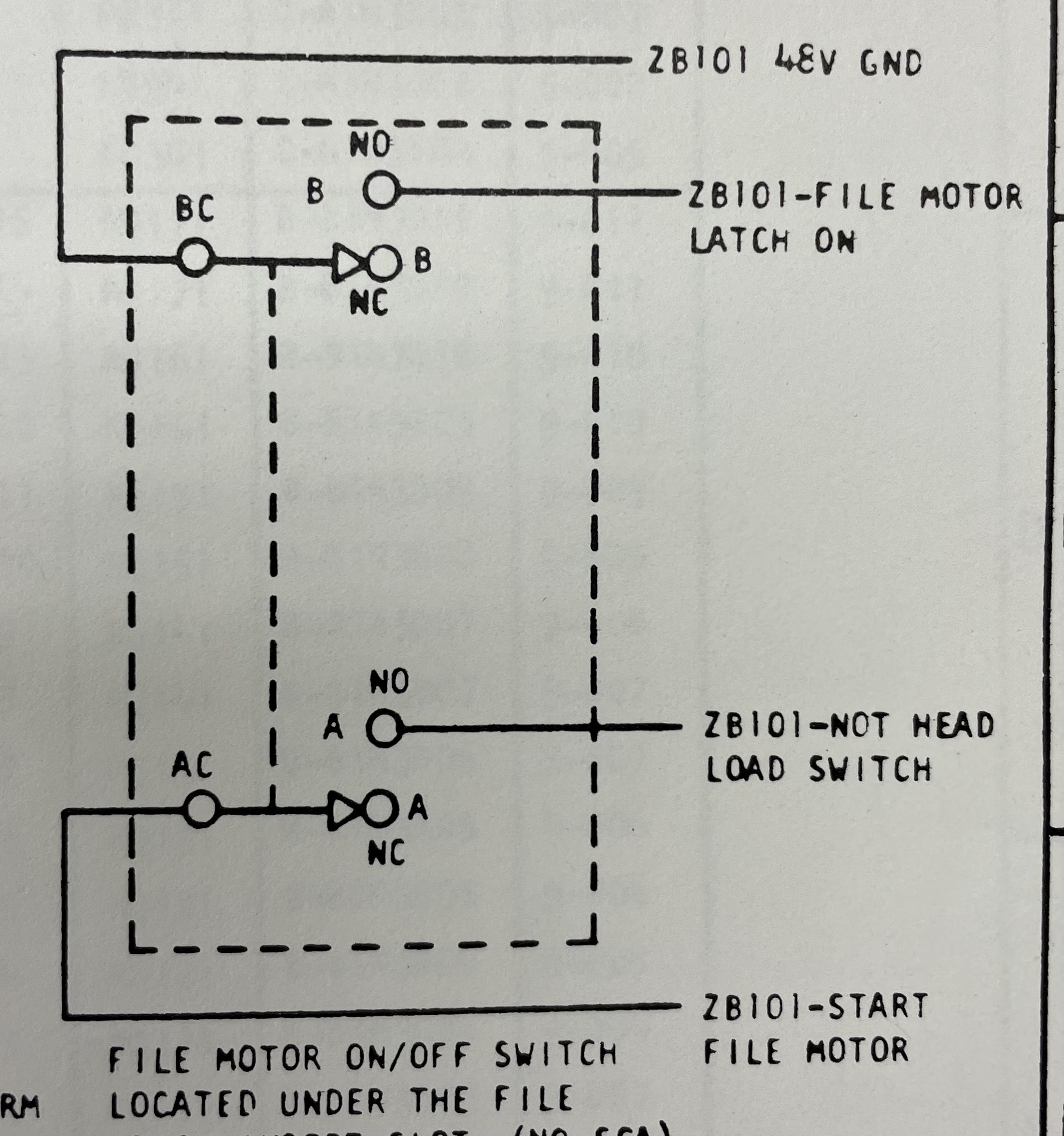
The disk drive starts the motor and waits 90 seconds to see if it has reached full speed. At that point, if the motor speed is good, based on the rate of sector mark pulses that are detected. then a solenoid is activated to load the heads.

That solenoid pushes a cam out into the path of the two head pivots, pushing the heads down towards the surface of the disk to cause them to begin flying. The motion also activates a "head loaded" switch that lowers the solenoid current to a holding level. 

The switch tells the drive that it is now ready for access. The drive has the arms out to the cylinder 0 location, called the home position. If the Read gate is turned on, the drive will emit clock and data bits corresponding to the selected track on cylinder 0, repeating the four sectors over and over. 

If the speed of the disk drops below 70% of target RPM or power fails, the solenoid drops which lets springs pop the heads up out of the way of the platter. A stored charge in a bit capacitor drives the arm movement mechanism to yank the arm all the way back off the platter entirely. 

INTERRUPTING THE HEAD LOAD BUT FOOLING THE CONTROLLER

I can remove the pivot pin so that when the head load solenoid activates, it turns on the 'head loaded' switch but does NOT push the cam out. The heads will stay spring loaded far above the disk surface, but the controller logic will believe they are down. It will then believe it is at cylinder 0 and waits for a Read Gate or Write Gate to command reading or writing at the current location.  

There was an alternative where we would use a switch to reroute the wiring from the solenoid to a fixed resistor, while sensing it and using that to override the 'head loaded' switch. I will look into this because it would make the drive even easier to switch between real cartridge and SD card access. 

INJECTING DATA STREAM AS IF THE HEAD WERE FLYING ON THE DISK SURFACE

IBM widely uses wired-OR junctions in their logic rather than an actual OR gate. This behaves similar to a shared bus. All the gates driving signals onto the wired-OR are open collector gates, which either pull the output down to ground or leave it alone. One pullup resistor makes the wired-OR sit at logic high level if all the driving gates are inactive, but any one or multiple of them can pull down to ground.

There is no penalty if more than one open-collector gate is pulling to ground. This is convenient because we can freely inject signals into these wired-OR structures without needing to add gates. 

The Read Gate is actually an open collector gate which pulls the wired-OR to ground when we are NOT asking for a read. Thus, it doesn't matter if the head circuitry is sending 1 or 0, the output is held constantly low. 

This is the place where we can take control of the read circuitry and send in our own data and clock pulses. Since the real heads are lifted by springs, not flying on the surface, they will not be generating any pulses. The line from the amplifier stays high, only going down to ground as pulses are generated to reflect a flux reversal on the disk surface. 

We will add a wire to this pin and, using an open collector gate, pull the line down to produce pulses at the points where we believe they would be emitted when reading a real disk. I don't need to modify any electronics or disconnect the heads; they remain ready to do their job if the head loading cam pivot is put back in place. 

WHAT WE NEED TO CAPTURE TO EMULATE THE DATA STREAM AT THE HEAD

In order to know what bits to send and when to send them, we must know where the heads would be flying at all times. To do that, we have to tap the disk access and position feedback lines so that we can mirror the movement of the arm, e.g. what cylinder we are on. We have to see the sector marks and the reference or index mark that defines the first of the four sectors. 

As the sector and index marks arrive, we calculate where on a track we are. A fixed time past the end of the sector mark is when we send the special sync word that follows a long stream of all zero bits. This allows the drive to separate the data that will follow into clock and data bits. 

We know the size of a sector (321 words of 20 bits) and the time it takes to rotate through it (10 ms) thus we can know exactly what word and bit is 'under' the head at any moment. Basically we have 1.55 bits passing per microsecond or 31 microseconds per word. 

The drive is sent three signals to control arm movement. It has a direction, to or away from the central hub, a step size which is either .01 or .02 inches, and a 'go' signal that commands the movement. The drive sends back a 'home' signal whenever the arm is at cylinder zero. 

The 1130 software has to figure out what cylinder it is currently accessing. The general method is to loop doing backwards steps until the 'home' signal is detected. It then adds for forward and subtracts for backward, either 1 or 2 cylinders depending on the step size. We will do the same to know what cylinder the real drive arm is sitting over. 

The drive is given a head select signal, choosing whether we are connected to the top or bottom surface for our reading and writing. We have to watch this signal to know which data the head would have been seeing. 

Finally, the drive is sent Read Gate or Write Gate signals when it thinks it has reached the target sector (out of four) for a given read or write operation. We are watching those signals so that we can begin generating the data and clock pulses at the proper time. We look in memory for the sector we are sending, since we know the cylinder, track and sector number. Based on time since the last sector mark, we know what word we are feeding to the controller. 

Data is written on the disk surface from the least significant bit (bit 15 for an 1130) to the most significant (bit 0), followed by a string of four bits that provide error checking. The error check is simply that the number of one bits in a word must be evenly divisible by four. If not, the extra four bits make this happen by sending 0000, 1110, 1100, or 1000 to round up. 

CAPTURING DATA WRITES 

The drive creates the write clock signals and sends them to the 1130 device controller logic, which in turn emits data pulses in between the clock pulses and only when the bit should be written as a 1. We can pick this off the backplane of the drive electronics, thus when we see the Write Gate activated and see the pulses come in, we can ignore the initial zeroes, ignore the special sync word, then capture each of the 321 words to write them onto the disk image. 

THE IMPLEMENTATION I INTEND TO CREATE

I expect to build this around a Digilent Arty S7 Xilinx FPGA module and an Arduino Mega 2560. The Arduino will manage the SD card, transfer the data via SPI link to the FPGA board when 'loading' or 'unloading' the virtual disk cartridges, while providing a user interface through an LCD display with buttons. The FPGA will watch the drive signals, model the movement of the arm and disk surface, thus it will produce the pulses during reads and capture the data during writes.

The FPGA module has RAM on the board which is what we access during disk operations, the full content of the disk cartridge having been loaded down to the FPGA from the SD card attached to the Arduino. Any writes to the virtual cartridge are stored in the RAM. When the physical disk drive is switched off (or power is lost on the 1130), the contents of the RAM are written to the Arduino and used to update the image on the SD card - an unload of the cartridge. 

Light panel mounting completed, installed and tested

FITTING THE CLAMPS AND HOLDERS FOR THE UPGRADE PCB

I made use of rubber gasket, formed as a U channel so that it could slid over the edge of the clamps and provide both protection and some thickness to be pressed down when my clamp is engaged. There is a clamp for each side. 

The clamp itself is fitted with one lip hooked on the front facing edge of the Lucite blocks of the panel, the other lip behind the PCB holding it pressed against the rear face of the honeycomb. A thumbscrew tightens the clamp into place. 

I did need an extra layer of rubber to get a firm fit, but everything is nice and tight, easy to get the board in and out. 

INSTALLING THE PANEL AND HONEYCOMB INTO THE CABINET

The Lucite blocks on the left and right side of the honeycomb have screw threads allowing them to be bolted onto the metal supports inside the cabinet. This places the display panel on the face of the cabinet and secures the assembly prior to fitting the lamps. 

I couldn't get a small screwdriver into one side of the cabinet, as it is restricted due to the Emergency Power Off (EPO) pullswitch and the terminal block for Lamp Test and AC Power. I had to remove the EPO plate and switch to get be able to screw in the lucite. 

The clamp on that side would not fit under the wire terminals going to my PCB, but with them removed temporarily the clamp slid right into place. The wires were put back and hooked to the PCB. 

WIRING THE POWER AND LAMP TEST WIRES

Heavy wire brings the common 7.25VAC power that drives all the lamps when they are illuminated. This is produced by a step down transformer power supply inside the 1130 which has one side of the output tied to the common signal ground, the other oscillating plus and minus 10.25V to produce the 7.25 RMS that illuminates the lamps during the positive going half cycles. 

There is also a Lamp Test line which is either held at ground or fed 3VDC. Resistors isolate each SCR trigger from this common line, allowing the individual signal lines to fire just one SCR while Lamp Test fires all the SCRs simultaneously. 

I provided three heavy clamping terminals to connect the AC, common ground and Lamp Test wires. These were wired over to the terminal block on the 1130. 

HOOKING UP THE SIGNAL LINES FOR THE INDIVIDUAL LIGHT CIRCUITS

A pin on the rear of the PCB is provided near each light position, to feed to the nearby SCR that controls that bulb. These are arranged in the same spacing and positions as used with the original IBM mechanism - horizontal boards mounting up to 16 bulbs and SCRs for a half row of the display panel. The signal wires have round push clips on them, which slide neatly over the pins on my PCB. 

I pushed them all on and had a completely installed board securely held in the cabinet. All was ready for testing. 

LAMP TEST AND COMPLETED PANEL WORKING PROPERLY

I fired up the IBM 1130 and flipped the Lamp Test switch under the top cover. All the bulbs lit up showing that the bulbs were all working. The switch is under the cover as part of the CE (Customer Engineer) group of switches that are considered service/maintenance tools. 

I displayed memory contents are some locations with known contents, then stepped through some instructions to verify that the register contents and system status is being displayed properly on the panel. I am preparing a video to load to my YouTube channel that will show the project and successful test.

Saturday, July 9, 2022

Missing handle for rear door latch - modeled in Fusion 360 and sent out to fab

REAR DOOR LATCH

A rear door on the IBM 1130, behind the disk drive, has a latch mechanism to release the door. This is used in order to swing up the top cover to access the Customer Engineer controls or to release the other rear door that exposes the logic gates. 

On this machine, the handle was broken off and missing. I was able to take apart the remainder of the latch assembly and reverse engineer the mounting method for the handle. 

DESIGN A REPLACEMENT USING AUTODESK FUSION 360

Armed with measurements of the mechanism and an idea of what handle shape would work, I then created a quick and dirty wood handle to test out the idea. When that proved acceptable, I opened up the CAD program Fusion 360 and designed the proper handle to be milled out of aluminum and with 4-40 threaded holes tapped in the rear. 

Rear side of handle with tapped mounting holes

XOMETRY.COM FOR FABRICATION

This was uploaded to two CNC services, Hubs.com and Xometry.com but with a total price just under $100 I chose the latter service. The part should arrive by the end of July, being fabricated overseas to save on the expense. 

Friday, July 8, 2022

Light panel glued together, once fully hardened the panel will go back into the 1130

PREPARING ASSEMBLY FOR UPDATED LIGHT SYSTEM

Lucite adhering to nylon honeycomb

Glue bond failed on this side

My clamp to hold PCB behind honeycomb

The Lucite must be glued to the honeycomb and the panel/honeycomb assembly screwed into the pedestal cabinet above the console printer, before the PCB with my lamps can be placed behind and the bulbs inserted into the cells. I had all the bulbs inserted into the PCB ready for the insertion. 

Bulbs inserted into front side of PCB

PARTS ARRIVED TO COMPLETE THE JOB

I had been waiting for a plastic glue, to affix the Lucite to the Nylon honeycomb, plus a rubber lip that would slide of the side of the PCB and fit into the steel U channels fasted to the Lucite blocks. When they finally arrived it was time to do the last bits of assembly. The glue-up was straightforward, held in place by a clamp until it dried. The rubber only needs to be cut to length and slid onto the PCB edge.

Glued but needs 24 hours to reach 80% of final strength

Thursday, July 7, 2022

Accelerating the sludge removal from the 1053 Console Printer

APPLIED NEW CLEANING METHOD

A fellow restorer has recommended that I soak the typewriter in a warmed bath of Simple Green, which won't damage the motor or solenoid enamel coatings. I picked up a large tub, aquarium heater and high capacity pump to agitate the solution, mixed up some cleaning solution and dumped the typewriter into it to see how it worked.

I had warmed the solution to 93 F, the max that my heater can be set to, before inserting the typewriter into the bath and switching on the pump. The water from the tap was already at 90 F and the sun on the solution pushed it up over 100 so I really didn't need the heater. 

Bathing in Simple Green with circulation pump

I left the mechanism submerged for a few hours before I pulled it out and disposed of the soiled solution. I carefully checked the bath for small springs or other parts before tossing it out, just to be sure that the water circulation didn't dislodge anything. 

The 1053 mechanism from the 1130 I am currently restoring was first into the bath. When it was removed, I tried to operate a number of mechanisms that had been frozen or sluggish before, such as the print cycle clutch and the carrier tabbing to the right. 

They moved! It does seem to work, in spite of its gentleness. I set up a table and a production line to soak my three selectric mechanisms - two 1053 console printers from 1130 systems and a Datel Model 30 terminal, which was sold as an alternative to the IBM 2741 terminal. Both of those are full typewriters that communicate over telecom lines, typically they were used as timesharing terminals. 

Mechanisms waiting their turn for the solvent bath

The two 1053 printers aren't yet perfect, but with quite a bit of grease removal I should have no problem getting them to 100% functionality. The one from the 1130 I am currently restoring was missing the rotate tape but I already had a new spare tape of the correct size. 

SELECTRIC CARRIER - SOME BACKGROUND READING

The carrier is an assembly that slides left or right on a round rail in the front and slides across a flat plate at the rear. Near that flat plate are two toothed racks. Levers on that back end produce a single step forward in a space operation, a single step backwards for a backspace, or latch the levers out of the way to allow the carrier to be pulled rightward until a projecting tab pin unlatches the lever to stop the carrier at an intended tab stop. 

The round rail in the front will rotate once for a print cycle, which imparts the motion to slam the typeball forward to that a spot on the ball strikes the platen through the ribbon and paper. Thus the lowest level on the carrier is a platform that pivots front and back to move the ball to the platen.

The type ball sits on a pivoting front to back subassembly which produces the tilt. That is, it leans the ball forward or back to put one of the four bands around the ball in position to strike the ribbon and paper. This is the top level of the stack - lowest pivot platform, middle rotation wheel and then the upper tilt assembly. 

In the middle on that pivoting subassembly is a wheel which rotates to move the ball so that from the top it is turning clockwise or counterclockwise. This wheel can be moved to one of five positions in either direction, thus there are 11 discrete rotations of the ball that are selected. Combining 11 rotations and 4 tilts gives 44 selectable characters. 

The wheel can be moved more dramatically to rotate the ball an entire 180 degrees, making use of a second hemisphere. This is a shift operation. Printing a character by picking which of the 44 on a hemisphere to slam into the ribbon is done during a single print cycle. However, to shift or move to the other hemisphere needs its own cycle prior to the actual printing of a character on the other side. 

Tilt and rotate are selected by tightening or loosening metal bands that run over pulleys on the left and right side of the typewriter, while being fastened to the carrier at each end. Thus, if a pulley on a lever is bent away from or toward the center, the effect is to move the tilt or rotate part in the carrier. One end of each band is fixed to the carrier itself, the other end of the band is hooked to the wheel (for rotate) or to the pivoting subassembly (for tilt). 

Early in a print cycle (one rotation of the print shaft), the tilting and rotating take place. The ball spins and tilts to position the character properly. Later in the print cycle, it slams the ball forward to strike the ribbon and paper. 

Additionally, parts move the ribbon up into position, leaving it down and out of the way so the typist can read the prior characters easily until it is needed during the act of printing the next character. On the 1053, the ribbon lift mechanism has two settings, controlled by yet another band. A plastic band is tightened or loosened by solenoids on the side of the machine to control how much the ribbon is lifted when it moves up for a print operation. Using a ribbon that is divided down its length with red and black inked halves, the variable lift can select the color that will be used for the typed character. 

A few other parts are here as well, adjusting the striking force for when carbon paper and multi part forms are used on the typewriter. All of these parts must be cleaned and move freely to have the typewriter work properly.

CORROSION CONCERN

I do see some corrosion on the rails that the carrier moves along. It does not seem to affect its operation but I won't know fully until I get everything freed up and working well. It is possible that these will need to be resurfaced or replaced. They are common to ordinary Selectric I typewriters thus spares can be found if needed. Look closely at the rough surface. Perhaps the bearings that slide along this are also galled internally. 

Worrisome corrosion on the front rail for the carrier

Wednesday, July 6, 2022

Taking advantage of cleaning process to handle all my Selectric printer mechanisms

SETUP OF THE BATH, HEATER, PUMP AND SOLUTION IS AN OPPORTUNITY

Since I will have prepared everything to dunk the 1053 printer from the machine I am restoring and remove stale lubricants, it is an opportunity to clean the other two mechanisms that I have. My own 1130 has a 1053 which is in much better shape than the restoration printer, but could still use a bit more cleaning. 

In addition to those, I own a Datel 30 terminal, a product built to compete with IBM's 2741 terminal. These use the Selectric typewriter mechanism and were connected over telecommunications lines to a remote computer to support timesharing and terminal access. Just as the 1053 makes use of solenoids and microswitches, these other terminals use them as well. 

While the 1053 is an output only device - a console printer - the 2741 and Datel 30 are both input and output, having keyboards as well as the typewriter output mechanism. This is even more firmly frozen than the 1053 printer, thus needs a deep bath before I can get to work on it. It appears to be in good shape with intact metal ribbons and other parts. 

Underside of the mechanism

Top view of the mechanism

1053 Console Printer - not an ordinary typewriter Selectric element (ball)

STRUCTURE OF A SELECTRIC TYPE ELEMENT 

The familiar 'golf ball' element from the Selectric typewriters is a metallic appearing ball that snaps onto the mechanism of the typewriter. Changing elements allows the typewriter to print with different fonts and special characters. This ball is actually constructed of nylon, colored to look metallic as IBM believed that a plastic appearance would be taken as a sign of cheap construction. 

The ball is a partial sphere, injected molded as two almost hemispheres then fused into the ball shape. Around the lower 'skirt' are teeth which allow the typewriter mechanism to lock the ball into precisely the right rotary position when typing a character. 

The center of the ball is the attachment point to the typewriter mechanism. One hemisphere is the regular or unshifted side, representing the lower character on keycaps, while the other hemisphere is reached by using the Shift key and thus will type the upper character on keycaps where there are two symbols. For letters, the two sides had lower case and upper case letters. Other keys had two symbols, e.g. the key with 1 on the unshifted hemisphere and the ! on the shifted side. 

A hemisphere is divided into 11 rotary positions from one edge to the other, these are termed rotations of +5, +4, +3, +2, +1, 0, -1, -2, -3, -4, and -5. The face is also divided into four rings that run left to right. The ball can be tilted to the 0, 1, 2 or 3 tilt level (T-0, T-1, T-2 and T-1,2), in addition to its rotation to one of 11 rotary positions. 

This combination of tilt and rotate places one of 44 positions on the hemisphere directly facing the ribbon in front of the paper and platen. You can see the raised letters on the element at each of these 44 positions. Fusing the two sides into a sphere provides the full 88 characters available on a type element. 

Note that this is for the original Selectric mechanism, sometimes called Selectric 1 to distinguish it from later versions that had balls with 96 elements in total for the Selectric 2, Selectric 3 and other families that came later. The 1053 is an original Selectric family member and uses the 88 character elements. 

TYPEWRITER ELEMENTS USE CORRESPONDENCE CODING

The ordinary Selectric typewriters of that era assigned the characters on the keyboard to various positions on the type element in a fixed way. That is, if you swapped a Letter Gothic element for a Prestige element, the same character was at the same relative location on the ball, although its typography was different to produce the different font type. 

On the correspondence elements, some sample characters and their positions were:

  • A   T2,  R -2
  • Z   T0,  R  0
  • 0   T0,  R +4
  • /    T3,  R -1

MAINFRAME AND TERMINALS HAVE ALTERNATIVE PTTC/BCD CODING

An older encoding system was used to encode characters for typing back in the 1401 computer era, where the 1050 terminal system initially used the Selectric mechanisms. These machines stored characters in Binary Coded Decimal (BCD) and on paper tape in PTTC code. The type elements produced for those older systems had the characters assigned in different locations on the ball. 

The 360 and all the Selectric mechanisms in the 1050 series (1052 and 1053) used the BCD encoding. IBM produced some Selectric based terminals, for example the 2741, that could be wired to either coding scheme. Famously, users running the APL language on a 2741 had to know which encoding the terminal was wired for, in order to install the proper version of the type element. These were the 987 and the 988 elements, for correspondence or BCD encoding respectively.

The same characters in the short list for correspondence are on the BCD ball at:

  • A   T3,  R -5
  • Z   T1,  R +4
  • 0    T0,  R  0
  • /     T1,  R -5
We can therefore see that the ball in its home position of zero tilt and zero rotate would produce a Z on the correspondence element and a 0 on a BCD element. 

THE TYPEBALL ON AN 1130 AND A S/360 CONSOLE

IBM Selectric Type Elements have a three digit code stamped on the nylon ball just under the lever on the top which identifies the font on the ball as well as whether it is correspondence or BCD. The ball on the 1130 is a 969 - "1131 & 1800 SYSTEM UC~UC" and the 360 console uses a 952 - "360 EXTENDED BCD"

Monday, July 4, 2022

Double checked the 1053 emulator before attachment to IBM 1130

CAREFULLY CHECKING THE 1053 EMULATOR BEFORE USE

I designed and built an emulator to plug into the 1130 for when the console printer is not operational. It is shared on Github as https://github.com/cclaunch/PC1053 which I am updating based on this checkout and subsequent testing with the computer.

I am not sure if this had been plugged into my IBM 1130, it may only have completed checkout with a test driver subproject. Any errors in my implementation are likely mirrored in the test driver, thus this warranted some careful validation before I will turn on power on the 1130. 

The first step was to verify from the 1130 ALDs that the connections on the SMS paddle cards are the signals I believed they were. I then beeped out these to the emulator to be sure I wired them to the intended pin of the Arduino or the intended terminal of the relay boards.

This design makes use of the open collector gates that IBM uses in the 1130 to drive the solenoids of the real 1053. These work fine with the pullup resistors built into the Arduino, thus I can directly hook these inputs to the Mega2560. 

I fired up the emulator without hooking it to the 1130. This let me inject various signals as if the 1130 were emitting them by simply tying that SMS paddle pin to ground. I verified that the relays and the signals they connect were in the proper idle state, including reporting that paper was now in the typewriter. 

All appears good, so it was time to connect this to the live 1130 system and begin debugging both my emulator and the device controller circuits inside the 1130. 

HOOKUP AND USE WITH THE 1130 - SOME COMPLICATIONS

The 1053 connects to the 1130 with three SMS paddle cards, two for signals and one for power. SMS cards have 13 fingers on the end of a phenolic printed board, labeled A through R from left to right. IBM named the two signal connectors PF1 and PF2, while the power connector is called PP1. 

With three otherwise identical SMS sockets, it would be important to get the proper paddle cards in the proper sockets. This is nothing unusual - nothing blocks putting an SMS logic card into a 1401 system in the wrong place, just as nothing stops someone from putting an SLT card in the wrong slot of a compartment on the 1130. 

However, it appears someone was unduly concerned, as IBM took extraordinary steps to protect against inadvertent misconnection. The power paddle card fits into a bank of sockets for power delivery that has a heavy metal bar spanning the H finger position of all sockets. Thus, the paddle cards for power have to notch out the card where the H finger would sit so that it can slide in, otherwise it is mechanically blocked. 

1053 power paddle card with notch 

I can understand a bit why the power sockets need protection - there is 230VAC, 115VAC, 48VDC and 12VDC delivered across those fingers which would be a bad thing to deliver to logic cards or the signal paddle cards. However, IBM didn't stop there. They could have put notches in different positions of the two paddle cards and their corresponding sockets, but they did not. Instead, they converted one of the two paddle cards to a hanging SMS socket. 

That spoils the purity of the SMS based signal connections. These are used for various peripherals - the 1053 printer, the 1134 and 1055 paper tape devices and the 1627 plotter. The block for these signal connections either has sockets installed or blank spacers for devices that are not configured on a particular system. The cards push into the block from the front and the sockets or spacers are all held down by metal rails which are bolted together at the ends. 

Except . . . the 1053 signals are a pair of reversed connectors - one socket and one paddle card on the CPU side and one paddle card plus one hanging socket for the 1053 side. One can't simply pull the socket off the card, instead you must remove the metal bars, take apart all the sockets and spaces, thus freeing the socket that is attached to the 1053. 

Signal cables PF1 below and PF2 above

Since these two blocks for SMS connections are down inside the bowels of the machine, behind the built in disk drive and just behind power supplies, you must swing out the logic gates and crawl inside the machine to connect or remove these cards. 

I now have an answer to my question of whether I had ever connected the 1053 Emulator to my 1130 system. I could not as I built the emulator with two paddle cards for signals and a regular power paddle card. No notch in the power card. No socket on the PF2 signal line, just a paddle card. 

Emulator with paddle cards for both PF1 and PF2

MAKING CORRECTIONS TO THE EMULATOR TO PERMIT CONNECTION TO THE 1130

I used a hacksaw and cutters to open a notch where the H finger was on the power paddle card, allowing it to fit into the 1130's SMS power connector block with its blocking metal bar. 

I found my spare SMS socket, one designed to take push on clips rather than wire wrap or solder. It took quite a bit of heat and technique to solder wires to those wide bars but I completed that, then soldered those wires into the paddle card for PF2. It is a bit clunky, but I can insulate and tie up the paddle card part and use the socket for the connection to the 1130's card. 

If this were going to be a regular peripheral connected to 1130 systems I would hunt down a proper hanging SMS connector and wire it up to the emulator, doing away with the paddle card and funny socket extender. However, I see this as a device to be used for intervals where the 1053 itself is off the machine being serviced, to be removed once the console typewriter is back in service.