SYMPTOMS VARY BETWEEN THE TWO CARDS BEING STUDIED
The primary card that was in the IBM 1130 when acquired by the owning museum exhibited on oscillation of the -Delay output signal, which is what is switching on the Run state and blocking further operation.
A backup card, scavenged from a donor machine they also bought, shows a repeated spiking -DC Reset signal. That means that the machine with the backup card is being reset over and over, thus unable to do anything productive.
CHALLENGE OF OTHER COMPONENTS ON THE CARDS
The cards are not only SLT cans, they contain other components as well. I have not found much documentation on those components and therefore it can be challenging to sort out what they do in a circuit.
RC (Resistor-Capacitor) Modules are the IBM name for many of these. I have also found discrete two-terminal parts that are inductors, capacitors and resistor, but space savings benefits come from use of RC Module thus they are plentiful on cards.
 |
| RC Modules between SLT Modules |
Since they are in circuit it isn't straightforward to put a meter on them to find their resistance or capacitance. A couple are labeled on documents I have for other cards and I know some of the values because of that, but most are a mystery.
I suspect that I will have to check these on many cards to build up a sense for the values of a particular RC Module. They are all numbered starting with 239, for example one RC module is 2390477 and that particular one I know from other documentation.
TRACING THE DC RESET LOGIC PATH
Since the DC Reset logic is smaller and more contained, I chose to debug this one first. The circuit does not have any external parts just connections between SLT can pins and the card pins. First we see the ALD description of the circuit with the AND-OR gate, the INT (debouncer) and entry from the button wire.
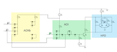
Now here is a schematic built with the three SLT modules that are used to build this - an AOXb, an AOI and an HPD shown from left to right. Essentially we have an AOI gate, with the output inverted again by the HPD, and an AOXb used as the second AND wired to the OR input of the AOI gate. Parts of the AOXb and AOI gates are not used by this circuit.
 |
| DC Reset circuit actual schematic |
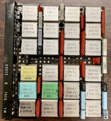
Finally we see a view of the card with the three SLT Modules highlighted.
 |
| Modules in the DC Reset circuit highlighted |

No comments:
Post a Comment