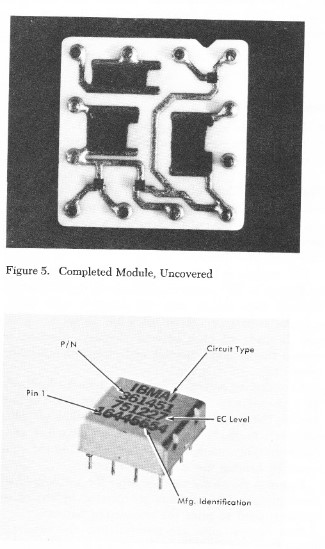
BASICS OF SLT
Solid Logic Technology is a packaging technique that places discrete transistor and diode wafers on a small square of ceramic, along with printed wiring and printed resistors These are then sealed and covered with a metal can.
 |
| SLT can |
The logic is mainly DTL - Diode Transistor Logic - where diodes are used to form the logical actions such as AND and a transistor amplifies (and inverts) the signal back to its target voltage levels. In some places IBM used ECL - Emitter Coupled Logic - for long signal runs or high power situations but their term for this is Current Switched. Since they invented ECL I guess they can call it whatever they wish.
Logic levels are nominally 0V for low and 3V for high. As with all logic families, there are bands of voltages which represent valid low and valid high signals, since it is unlikely to achieve exactly 0 and 3 due to resistances, other loads and similar electronic factors.
In between the lowest voltage for a logic high and the highest voltage for a logic low is a forbidden band that provides separation for clearly detecting which state we are in and to provide some immunity from noise in the circuits.
The output of a gate is set to provide a wider separation to allow for losses as the signal is connected to other gates. Thus, a gate will provide a higher guaranteed minimum voltage for logic high and a lower guaranteed maximum voltage for a logic low.
The SLT circuits are powered by three standard voltage rails - +3V, -3V and +6V. Thus the standard pin layout for the small SLT cans has four terminals in the center that deliver +3, -3, +6 and ground connections. The standard assignments on the SLT boards hooks up the rails, for example +6 is always on pin B11 and ground is always on pin D08.
THERE IS NOT A 1 TO 1 ASSOCIATION OF LOGIC GATE AND SLT CAN
Making the reverse engineering a bit more challenging is the fact that an SLT can may be a portion of a gate or often portions of several gates. Thus, a SS (Single Shot pulse generator) gate consists of portions of a FDD can and one SS can, plus several resistors and capacitors external to the cans but mounted on the SLT board near the cans.
The FDD can is four dual diodes - that is all it is. One of the dual diodes is used along with an SS to form the Single Shot circuit. The other three dual diodes may be used for different logic gates on the same card.
The workhorse gate of SLT is the AOI, which is AND-OR-INVERT. It has a set of diodes that isolate inputs so that if any of the inputs is low, the point where the diodes tie together is pulled down, otherwise it goes high. In other words, if all inputs are high then the tie point is high, otherwise it is low. The definition of the AND function.
 |
| AND-OR-INVERT can |
Then there are diodes hooked past the tie point that will provide a high level to the transistor even if the AND side tie point is pulled low. We can get a high to the transistor either way, from the OR input or from the AND function, thus it is an OR after the AND. Finally, the output of the tie point is passed through a transistor to invert it. This inverts the operation before, so that the AND function becomes a NAND and the or function becomes a NOR.
IBM refers to these in both the normal and inverted logic sense, as the functions are mirrors of each other. It can be shown as a block with four normal inputs and the output has an inversion symbol, the block labeled A. It can also be shown with four inverted inputs and an normal output, with the block labeled OR. In either case, if any of the four inputs is low the output is high, otherwise the output is low.
The AOI is made more extensible by providing a pin where additional diodes can be hooked to make the AND function larger than four inputs. Another pin adds additional diodes for more OR conditions to drive the gate. In support of these extensions, IBM provides blocks of diodes in an AOXb (AND-OR Extender) can.
 |
| AND-OR extender can |
AOI has a single gate on the can. The AOXb has two dual-input and one quad input extensions, thus can be used with up to three gates. The basic not circuit is an II, Isolating Inverter, which provides two not gates per can.
 |
| Dual NOT gate can |
Other cans on our board include the HPD, High Power Driver, which can drive 70mw of power and has two independent drivers. There is an AI which is an AND-INVERT without the or connection. The workhorse of state machines is the flip flop FF can which IBM also calls a multi gated trigger. There is one FF per can.
 |
| FF can |
The input gates are unusual as they are what IBM calls AC coupled inputs. Lets look at pins D and E for our discussion. If pin E is at logic low level, then whenever pin D transitions from high to low (a trailing edge), the flipflop is triggered to its reset state. However, if pin E is at logic high level, the resulting pulse when pin D has a trailing edge will be absorbed through pin E and does NOT trigger the gate.
These are drawn on IBM block diagrams as an inverted input which is called the gate and an input with an N which is the AC input or trigger. While a gate input is low, a transition on a trigger input will set or reset the FF (depending on which side of the FF it is placed). When the gate input is high , triggers are ignored. This gate has a gated trigger at D/E for reset, another gated trigger at A/B/C and in 3 is an extender to add even more AC trigger inputs. Similarly, J/K, F/G/H and pin 8 are AC triggers and extensions for the set side.
Pins 11 and 4 provide the output and inverted output of the flip flop. Pin 7 and pin 12 are direct reset and set links, called DC Reset and DC Set, usually they would be connected through diodes such as with pins 1 and 2.
No comments:
Post a Comment