BUZZED OUT THE CAPACITOR THAT WAS SHORTING 4MHz CLOCK TO GROUND
I found the capacitor which had one end connected to the AREF external connector of the board. Given its relatively large capacitance, its impedance at the clock frequency of my SPI link was nearly zero.
REMOVED FROM BOARD AND HOOKED TO SCOPE
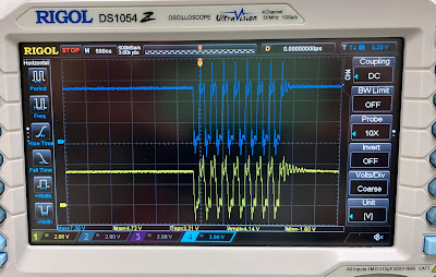
It was quickly desoldered. The repaired board was taken to the bench and the scope connected to the AREF external connector pin which was now wired to the SPI clock for USART 2 on the microprocessor. If the clock was now working, with the scheme I put in place there should be bursts of 16 clock cycles every second or two while my Arduino looped around sending alternating commands to the FPGA.
CHECKED WITH THE LEVEL SHIFTERS TO PROVE THEY CAN HANDLE FREQUENCY
I also connected this through the level shifter boards I will be using, as I needed to be convinced that the shifters could operate with a 4MHz signal. The results were great! The clock from the SPI link clearly showed up on the scope in bursts of 8 cycles with the rest state high.
The voltage of the Arduino produced clock swung between +5 and 0V, while the output of the shifter moved in concert between +3.3 and 0V. The waveform was not distorted too much, a possible outcome if the shifter couldn't handle the 250ns cycle time and 125ns duration of the 'on' phase of the clock. All was good with the signal quality and levels.
ONE ISSUE TO RESOLVE, OTHER THINGS TO VERIFY NEXT
What was evident immediately, however, was that I was NOT getting the 16 bits I expected during the SPI transaction. The ATMEL documentation made it sound like the buffered USART would accept two bytes and send out both in one transaction, but that is not what I am seeing on the scope in real life. This could be a C coding error or a misunderstanding of the documentation.
In addition to that, there are several other things that must be verified to ensure that both ends are able to communicate. These include clock polarity, clock phase, and endian-ness of the transmission. I can change these at the Arduino to ensure a match with the FPGA but they must be verified and adjusted in necessary to have a good link.
Polarity for an SPI clock is whether the idle state of the clock is high or low. I want high and that is what I see on the scope, so clock polarity passes muster.
Clock Phase is a design choice for when signals are sampled - rising or falling edge of the clock - and as a consequence when they can be changed from one bit's value to the next. I can only verify this by watching the MOSI line, where the master (Arduino) sets up the 1 and 0 values of the bits in relation to the clock.
The Arduino takes a parallel word input to the SPI channel and shifts out bits one by one. What we need to see is whether it should put the most significant or the least significant bit out first. The goal is to have the assembled word in the FPGA match what we expect, not be swapped back to front. Again I can observe this by watching what the SPI channel outputs on MOSI and SCLK from the pattern I am writing

Apparently, the new name for MOSI is PICO (Peripheral In Controller Out). According to Peter Viscarola of https://www.osr.com/developers-blog/. This is a difficult issue for many. I may be 71, but PICO (and MISO becomes POCI) work for me. I've been waiting for some good, meaningful alternatives. And finally they arrive..
ReplyDeleteDon't forget Peripheral Select for the SS line
DeleteActually, the SS line becomes the Chip Select line.
Delete