Friday, May 6, 2022

Power problems ironed out, continuing both system and card debugging

WORKING ON THE SLT CARD TEST RIG AFTER DIGGING INTO ONE FAILURE I SAW

When I was running the card in Single Storage Cycle mode (SMC in some documentation for Memory Cycle), it should reset the Run flipflop when T7 clock state occurs. Specifically, the signal -T7 is fed to an edge triggered circuit, so that if the circuit is gated by a logic 0 on -Single Storage Cycle, it will sense a pulse to zero on the DC Reset input of the Run Flipflop. 

A similar failure occurred when a second circuit, also fed -T7 as a trigger, is gated by a logic 0 on -Wait Not Stor Load/Display. These two edge circuits are both implemented on a single RC Module (type 2390709) which has 33pf capacitors from the trigger and a 2.5K resistor from the gate, both feeding to a central point that is the output which is wired to the flipflop DC reset pins. 

I put the scope on the outputs of the module and saw nothing when the trigger went low. I pulled the module out of the card and checked its components, but it was solid as could be. I then checked all the diodes and transistor junctions in the Run flipflop but they too looked correct. 

RC Module removed from board

2390709 RC Module

Unlike other signals fed to different edge triggered gates, T7 is one of the few complementary signals where both the positive and inverted sense of the signal are fed to the card simultaneously. There is a +T7 and a -T7 input pin on the card.

For the complementary signals, I was feeding them from a pair of DIP chips on my breadboard - a hex inverter and a hex buffer - so that one input to the pair of chips would generate the complementary states as output. When I looked at the logic 0 output levels of those chips, I found that it was just above 0.3V. 

As a test, I hooked -T7 to a switch that directly connected it to ground when activated. The edge trigger fired and the Run flipflop was reset! My test setup was not pulling the node attached to the capacitor far enough down to create the desired output. 

I pulled out a relay board and used that to generate the complementary high and low logic levels for each of the complementary signals that are used with edge triggers inside the card. That did the trick and I was able to walk the card through all its paces. 

I carefully tested that each input caused the appropriate behavior in the card. A number of conditions cause the machine to take multiple T7 steps before starting the next memory cycle. Among them are arithmetic, shifts, and some cases of conditional branches. When any of these exist the machine does not start on the next memory cycle (at T0) until the condition is released. 

The machine will stop when a parity error occurs or when the CPU is stopped by the stop latch. This can be due to the Immediate Stop operator button or a wait instruction. The stop is processed at the end of a instruction cycle after the machine tests for any pending interrupts. The -Set Interrupt SP signal triggers the check of the stop condition; that worked perfectly as well. 

If the machine is stopped but an interrupt request arrives, it should go into Run state to execute the interrupt handler. This is triggered by the -Interrupt Request signal and it checked out when tested. 

When the Program Load button is pushed, circuitry will block the Run condition from coming on for instruction execution, but the machine is taking storage cycles to store the boot instructions coming from the boot device. These are triggered by pulling the -Delay output low (signal -Prog Ld T7 Phase B)

The block is released when a response arrives from the boot device that the data is complete. For paper tape it is a particular hole pattern, but for the card reader it is the end of the one boot card that signals completion. Relieving the block causes the processor to fetch an instruction from location x0000 and execute it. The block is -Prog Ld Not SRP or PT Resp (note an old internal name for the 1442 card reader is SRP). 

An additional signal that will stop the machine from advancing from T7 to the next storage cycle at T0 is the signal -CS Levels. Cycle Steal is IBM's name for direct memory access, which is managed by a second clock ring X0 to X7. This signal blocks the T clock from running while the processor is accessing memory using the X clock.

WILL DO FINAL FULL SPEED TEST OF CARD TOMORROW

I will hook the card up to the 2.25MHz square wave output of my function generator and test out is functions once again, just to be sure we don't have any subtle failures that only occur with brief pulses. I should see the +Phase A and +Phase B signals being emitted, the -T Clock Advance Sample and -T Clock Adv SP signals come out each time the T clock should advance, and suitable pulses be emitted for the -Phase A SP A output. 

Once that works, any problems with the Run condition staying on has to be caused by one or more of the inputs to the card, which I can quickly run through using the oscilloscope. 

I PLAN TO BEGIN TESTING THE SPARE CARD IN THE TEST RIG

Since the failure I saw in the spare card, failure to respond to the Prog Start complementary signals, might be similar to the issue I fixed with the relay modification to my breadboard, I will retest to see what persistent errors exist and debug from there.

REPLACED FUSE HOLDER AND REINSTALLED POWER SUPPLY

My local hardware store had panel fuse holders in stock. In short order I replaced the holder, inserted the fuse, reinstalled the supply and wired it up. 


DEBUGGED AND FIXED LACK OF +12V TO SYSTEM

The failure was clearly on the SMS power validation card, relay RR-1 which is triggered and holds itself energized when the three power rails (+3, -3 and +6) are present. That has contacts that energize relay R2 inside the power distribution box. That larger relay switches both +12 and +48 voltages onto the logic gates of the machine. 

Without this relay engaging, we don't get the voltage needed to properly sense the operator control buttons and mode switch. Nor do we have the voltages needed to read and write core memory, thus it is a good thing that we don't have the clocks running. 

When I received the machine, some prior restorer had replaced an IBM reed relay on the SMS power sensing card with a solid state DIP replay. I tested the IBM relay, found it good, and returned the card to original state. 

Unfortunately, the relay was misleading me and has failed (again). I restored the solid state relay and verified that the card now produces the right signal indicating good power levels. 

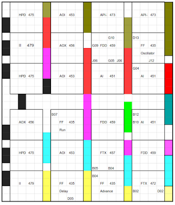
TWO PAGES OF ALD FOR THIS CARD ARE BELOW, FOR THE CURIOUS


Thursday, May 5, 2022

Did some testing of two cards with the newly built test rig, continued slowly chasing signals to pins for reverse engineering the cards

FINISHED SETTING UP THE TESTING RIG

I soldered and assembled the last 11 banana to breadboard jumpers, then wired up everything for testing this card. That involved several signals which are paired opposites (e.g. +T7 and -T7) so that one switch would flip both through the use of a buffer and inverter pair. 

I discovered that the mode switch and pushbuttons have an odd circuit that does NOT use SLT logic levels. The switches are connected to +12V, through a 470 ohm resistor to the logic card. On the card, the 'Z-INT' gate has a 470 ohm resistor to ground and a capacitor whose far end is hooked to -3V. The junction where the signal arrives also has a 1.2K resistor bringing the signal to the SLT logic gate that will be driven by it. 

The two 470 ohm resistors form a voltage divider giving +6V at the junction when the switch is connected to +12V. When not connected it is pulled down to ground. The SLT logic gate doesn't really care what the high voltage is, within limits, but provides a current flow down to any voltage lower than 3V such as the ground state of an un-activated switch signal. 


I had to pull out another power supply and feed 12V through 470 ohm resistors to the two signals that connect to Z-INT gates on the card - the +Single Step Mode and the -Reset Key signals in this case. With it wired this way, the cards responded properly to the state of these two buttons. 

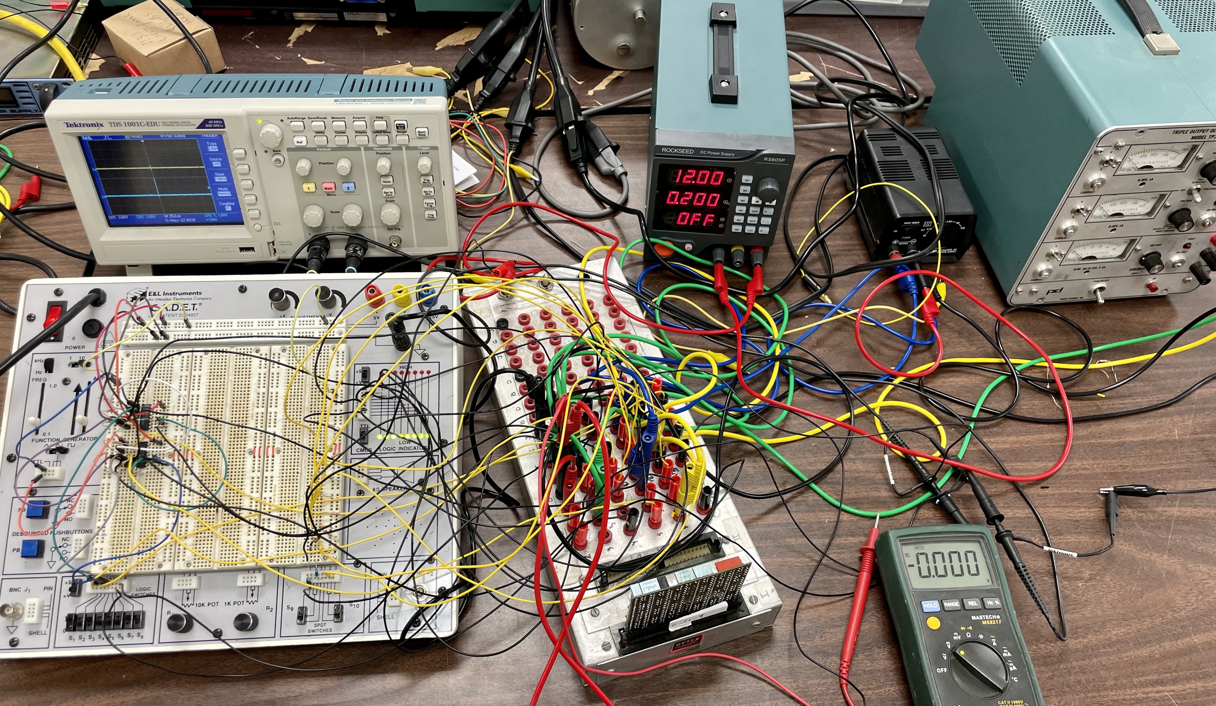
I used the 100KHz oscillator of my CADET breadboard machine to drive the card and had nine switches and eight display LEDs set up. Additional circuits were monitored on my oscilloscope. 

Test setup

INITIAL TESTS OF CARD 1 (FROM THE MACHINE)

I had a methodical set of test steps, beginning with testing the proper generation of system reset (DC Reset signal) both from the Power On Reset signal and the Reset Button activation. My second set of tests were to put the card in Single Step Mode and verify the proper state outputs include Phase A and Phase B clock signals. 

I quickly determined that this card is not responding to the Program Start Key signals at all. I verified that the matched pair of opposite inputs are produced as I activate on of the logic switches on the breadboard, but the card doesn't respond at all. Since it doesn't respond in several modes, which involves different sets of logic gates, the defect must be early in the chain.

I couldn't test any further without the ability to put this in various modes and trigger the Run state. 

INITIAL TESTS OF CARD 2 (FROM THEIR SPARE CARD COLLECTION)

This card behaved better in that it did respond to reset conditions and to the Program Start Key signals. I put it through its paces and found it well behaved in Single Step Mode. I seemed to work okay in Single Instruction Mode, where the signal -T7 Count 0 going off triggers the Run flipflop to turn off. 

However, when I tried to step it in Single Storage Cycle mode, which resets when T7 is reached, provision of the proper T7 signals did not reset the flipflop. 

Another path that requires T7 is recognition of the CPU Stop Latch. That is only checked at T7 time, as otherwise you would not complete the writeback of a memory word contents. The machine never responded to the CPU Stop Latch either which again points to failure of the T7 detection.

I felt that I could do some limited debugging with this card in the machine as long as I had it in either Single Step or Single Instruction modes. However, when I powered up the machine, I found that the lights on the keyboard did not illuminate (such as the Run state) and the machine was frozen.

A bit of debugging with the scope showed me that the Reset button signal was low, when it should be powered by +12V when inactive. I found that the 12V supply was not present anywhere in the machine.

NO 12V TO POWER BUTTON AND MODE SWITCH SIGNALS

My first investigation was to remove the small fuseholder on the power supply that protects the 12V generating transformer. The fuse came out and was good, but I couldn't get it back into the holder. The holder inner contact was twisted and bent in a way that blocked fuse insertion. I pulled the power supply again in order to replace the fuseholder. 

TRIED TO PROVIDE 12V WITH A BENCH SUPPLY, BUT IT DIDN'T REACH LIGHTS

My bench supply can deliver the 4A of 12V that is the capacity of the supply with the broken fuseholder. I applied power but there was no draw at all on the supply. The machine has a relay that only connects the 12V and 48V once the other power supply levels are verified by the SMS power sensing card. Something must be wrong with this - investigating tomorrow. 

Wednesday, May 4, 2022

Installed T3 transformer, continued on reverse engineering card, setting up testing rig to validate SLT cards

 T3 TRANSFORMER TO POWER CONVENIENCE OUTLETS IN 1130 SYSTEM

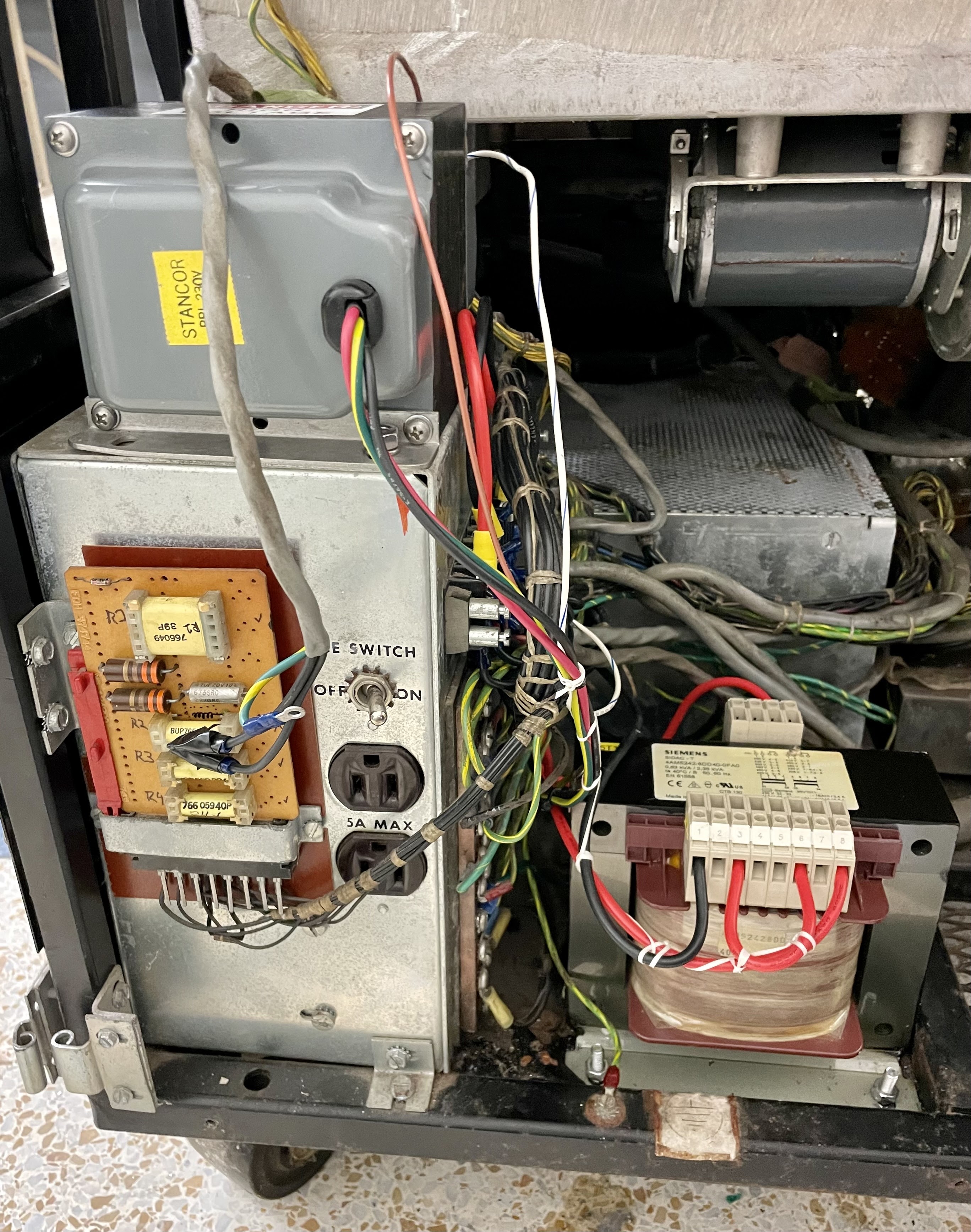
I picked a location for the transformer, where IBM would have one mounted in a suitably configured 1130 system, drilled holes and mounted it firmly. I then wired it into the system and laced up the wiring for neatness. The fuses for this circuit can be returned to their original sizes now.

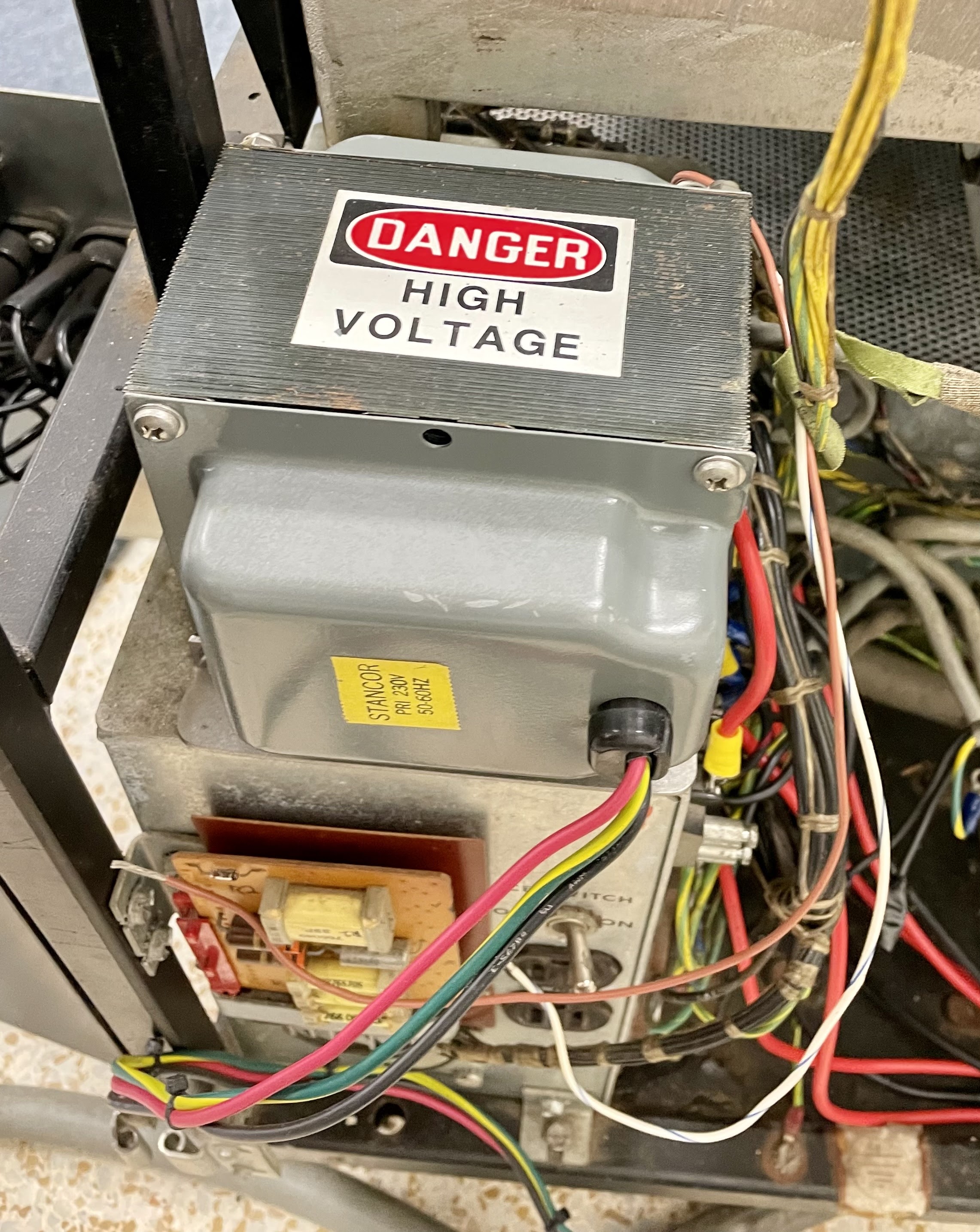
T3 in lower right and T2 upper left

TEDIOUS WORK FINDING CONNECTIONS ON THE CARD

Since there are 21 rows of 26 columns on the double size SLT card, the number of combinations to test in order to discover every connection is massive and infeasible to perform blindly. The situation is slightly better than it appears - not a combination of 2 items from 556 possible points - due to some points we can exclude.

The first row is used to mount the power rail filter capacitors and to carry some card pin signals over to the opposite side of the card, thus we can ignore those 26. Each of the SLT modules has four pins in the center which are used to connect the power rails and ground, so they can be excluded as well. This gives us 96 more points to ignore. 

Therefore we are looking for the number of combinations of two points selected from the 424 possible signal points. There are 'only' 89,676 blind tests to perform. That number can be further reduced by awareness of unused pins on specific SLT modules, and by excluding some open spaces between the SLIT modules when there is no other component mounted. 

That might get us down below the 50,000 neighborhood of tests. At 3 seconds per test, that would require around 42 hours of continuous work. I don't think I could work at that pace anyhow, but this is well into the impractical tedium zone. 

MAPPED OUT ALL THE RC MODULES USED ON MY CARD

I did manage to finish mapping all the components - with a bit of ambiguity that remains because a) in-circuit testing can produce invalid measurements due to effects of connected components and b) a pair of pins may be connected on the SLT card but not actually connected in the module. 

MAKING USE OF MY BREADBOARD SYSTEM TO HANDLE SLT 3V SIGNALS

I have an E&I CADET breadboard system which has some very convenient features for working with SLT. In addition to a standard TTL +5V power rail, it has variable positive and negative power rails which I can use to generate 3V for compatibility with SLT.

It also lets me set up the logic switches and the signal display LEDs to operate with either +5V or my variable (3V) supply level, so I can use these to create inputs and show outputs without building any interface circuits. 

BUILDING MORE BANANA PLUG TO BREADBOARD JUMPERS

A double SLT card has 48 pins but 8 of those are standard power connections (and for this particular card there is an additional pin used to increase current capacity for the +3V rail). Four pins are not used on this card, thus we are left with 35 input or output pins that I have to connect to test properly.

I will the using the breadboard to source and sink the connections, either setting inputs to static levels or using switches, while displaying the outputs. To make this work, I need jumper cables with a 22 gauge wire on one end and a 4mm banana plug on the other. 

The process of creating them involves, removing the covers, cutting and stripping wires, soldering wire to the plug, then reinstalling the covers - repeated for each jumper. I have 29 jumpers completed and have already cut and stripped the wire for the final 11 I intend to build. 

I also purchased more stackable colored banana plug to banana plug jumpers, since I need a pair for each voltage rail at a minimum plus the ground wires running to and between supplies. 

SET UP TO PRODUCE THE ALTERNATING CLOCK INPUTS TO DRIVE THE SLT CARD

The clock inputs to the SLT card I am troubleshooting must be a pair of signals of alternating phase, not just a single ended clock. I chose to produce that by setting up a 74ALS05 and a 74ALS35 chip on the breadboard. These are inverting and noninverting hex gate DIP chips that are pretty ideal to feed a square wave and get out a pair of out of phase signals to send over to the SLT card. Being open collector chips, they are magically 3V SLT compatible even though the chips themselves operate on 5V.

Breadboard with twinned hex gates for clock signal

My breadboard system can generate a square wave up to around 100KHz, not as fast as the clock in the 1130 but suitable for initial debugging of the card. I can switch over to my function generator that will produce a true 2.25MHz square wave for full speed verification. 

Tuesday, May 3, 2022

Slow progress reverse engineering the card, wiring in T2 stepdown transformer and replacement transformer for usage meter

BECOMING METHODICAL ABOUT NUMBERING THE RC MODULES FOR DOCUMENTATION

I came up with a naming scheme for the 30 non-SLT module components on the board, using C1 to C8 for the discrete capacitors and P1 to P22 for the other 2 to 6 pin components. I named the various modules and kept track of both the part number (e.g. 2390302) and the location of pin 1 for that module, since some are installed in the reverse sense to the others. 

As I learn about the components inside, their values and the wiring, I am writing it down as it makes the process of reverse engineering the board easier. So far I understand five of the ten part numbers; the goal being to document all of them in order to fully understand the circuit and find any defects.

INTERESTING OBSERVATION ABOUT IMPLEMENTATION ALTERNATIVES

The logic for resetting the Run flipflop is a set of conditions determined by edge triggered AND gates, all fed together with the DC Reset signal into an OR gate which in turn will drive the flipflop reset pin. That is how the ALD is drawn and what it suggests. 

Seemingly six AND gates and a 7-way OR

Instead I discovered that some part of the OR gate is actually making use of separate reset pins on the flipflop circuit. I am not sure how the rest of this will be wired, but the lack of an OR for these two signals surprised me and in some cases lack of an AND gate as we know it. 

This was during my investigation of the two cases for reset driven by the -Single Storage Cycle mode and when the system is in a wait (except for when the Mode control is on Storage Display or Storage Load). These are two edge triggered AND gates which use those states as conditioning gates and trigger when the machine reaches T7 clock state (on -T7 falling edge). 

Edge triggered gates are implemented with a front end that has a capacitor hooked to the trigger signal and a resistor from the other side of the capacitor that is hooked to the gate signal. Taking the gate signal to ground sensitizes the output so that a falling edge on the trigger will pass through as a pulse. Usually these are hooked to a diode on a gate such as AOI or AI. 

In this particular case, the two edge triggers are the same signal, -T7 and thus two capacitors in the RC Module 2390709 are wired to this signal via pins 3 and 4. The other side of the two capacitors are at pins 2 and 5. This RC Module implements a 2.5K resistor between pins 1 and 2, and another between pins 5 and 6. 

The RC Module used for these two 'gates'

Therefore, with trigger signal -T7 hooked to pins 3 and 4, the gating signals -Single Memory Cycle and -Wait Not Strg Load/Display are hooked to pins 1 and 6. the output of the edge triggers are pins 2 and 5, in between the resistor and capacitor. 

Rather than these being routed to a AOI gate, then the result of the AND routed to the OR gate on the ALD, these two pins of the RC Module are directly wired to the flip flop pins 1 and 2, which are DC Set/Reset inputs. When either of the triggered conditions occur, it pulses the Run flipflop to reset. No OR gate involved, other than the reality that a flipflop with multiple input connections inherently implements an OR where any of those inputs will cause a reset. 

Notice DC Set/Rest pins 1 and 2 in upper right

I am sure I will find other clever implementation details which save parts compared to the brute force direct implementation of the ALD circuit.

BOLTED DOWN T2 TRANSFORMER AND WIRED IT IN

Transformer T2 provides 115VAC power for a limited number of loads in the 1130 computer - incandescent lamp power supply, selectric printer motor, customer usage meter and future expansion with peripherals that have 115V requirements. The Stancor transformer at 750 VA capacity is suitable for this. 

750VA capacity stepdown transformer

I decided to mount the transformer right on top of the AC power distribution box, in a space that IBM has used for similar transformers. I drilled some holes and bolted it down well. The wires were trimmed and had ring terminals applied so that they could be wired into the terminal block where T2 connects.

Transformer being mounted above AC distribution box

WIRED IN THE REPLACEMENT TRANSFORMER FOR 40VAC FOR USAGE METERS

The small transformer inside the Customer Usage Meter power supply had self-destructed due to being fed 230V across its 115V taps prior to arriving at my facility. When I corrected the wiring transformer succumbed to its prior injuries, emitting some magic smoke in the process.

Post-smoke view of the old transformer

I sourced a suitable transformer to produce 40VAC which is what the usage meters require. It was slightly larger but I could fit it in to the housing and began to wire it into place. This power supply also includes some relay boards that switch between the Customer and the CE meters based on the setting of the CE keyswitch. 

Replacement transformer for 40VAC

It also runs the meter only when the processor and peripherals are active (the Run condition is on).  The small board with the relays and its wiring will be replaced in the housing and have the transformer output connected, just before I remount the power supply box inside the 1130 chassis. 

Wiring transformer into the power supply housing


Detailed tracing of DC Reset logic, different defects in the two 6213 cards

SYMPTOMS VARY BETWEEN THE TWO CARDS BEING STUDIED

The primary card that was in the IBM 1130 when acquired by the owning museum exhibited on oscillation of the -Delay output signal, which is what is switching on the Run state and blocking further operation. 

A backup card, scavenged from a donor machine they also bought, shows a repeated spiking -DC Reset signal. That means that the machine with the backup card is being reset over and over, thus unable to do anything productive. 

CHALLENGE OF OTHER COMPONENTS ON THE CARDS

The cards are not only SLT cans, they contain other components as well. I have not found much documentation on those components and therefore it can be challenging to sort out what they do in a circuit.

RC (Resistor-Capacitor) Modules are the IBM name for many of these. I have also found discrete two-terminal parts that are inductors, capacitors and resistor, but space savings benefits come from use of RC Module thus they are plentiful on cards. 

RC Modules between SLT Modules

Since they are in circuit it isn't straightforward to put a meter on them to find their resistance or capacitance. A couple are labeled on documents I have for other cards and I know some of the values because of that, but most are a mystery. 

I suspect that I will have to check these on many cards to build up a sense for the values of a particular RC Module. They are all numbered starting with 239, for example one RC module is 2390477 and that particular one I know from other documentation. 

TRACING THE DC RESET LOGIC PATH

Since the DC Reset logic is smaller and more contained, I chose to debug this one first. The circuit does not have any external parts just connections between SLT can pins and the card pins.  First we see the ALD description of the circuit with the AND-OR gate, the INT (debouncer) and entry from the button wire. 


Now here is a schematic built with the three SLT modules that are used to build this - an AOXb, an AOI and an HPD shown from left to right. Essentially we have an AOI gate, with the output inverted again by the HPD, and an AOXb used as the second AND wired to the OR input of the AOI gate. Parts of the AOXb and AOI gates are not used by this circuit. 

DC Reset circuit actual schematic

Finally we see a view of the card with the three SLT Modules highlighted.

Modules in the DC Reset circuit highlighted

Sunday, May 1, 2022

Working on sheet to document the destinations of card pins on the SLT modules and other components

 WORKSHEET SO FAR


The grid has one box for each of the potential holes in the board where components mount - in real life they are .125" apart, a bit larger on this image. An SLT module fits on a 4x4 space, which I mark with thin borders. There are 12 signal pins around the perimeter and the center block of four are the power/ground pins 

I also marked the type of module and the last digits of the module code. A flipflop (MGTR) is 361435 for example. With the flipflops, I wrote the name that they have on the ALD page. 

The two single shots are implemented by the FDD and FTX modules on the right column, bottom two rows. The outputs are on pins 2 and 9, where I wrote the card connector pin B02 and D02 that are wired to these points. The Delay flipflop has a connection to card pin D05 where signal -Delay is output. 

I haven't finished marking all the inputs and outputs yet, but this is a documentation method I will make use of for my overall work with the card. I can then make versions of this with the connections marked that complete some gate or set of gates where I am debugging. 

As an example, the single shot involves half an FTX, half an FDD, plus some resistor packs, a capacitor and an inductor. The input pin to the single shot would be shown going to the output of some interior gate on the card which drives the SS. 

Tracing SLT card pins to components, part 2

CONNECTION TRACING STRATEGIES

Inputs usually go to a diode either in an Add-Invert type of gate or to additional diodes that are housed in AOXb (And-Or-Extender) or FDD (Four Dual Diode) modules. Some inputs are edge triggers, so these will go to a capacitor which in turn feeds a gate.

High fan-out signals will be produced by HPD and AI-3V circuits, so I will check back from these to the pins most likely to have those fanouts. 

Once the external signals are tied to specific SLT modules, I can look at the appropriate other pins of those modules and figure out where they run. 

TESTING A BIT SLOW DUE TO FLAKY BANANA PLUG JUMPER CABLE

I was having difficulty finding the signals using the continuity tester, at first thinking I had oxidation on the banana sockets of my test setup, but I realized that the jumper cable was undoubtedly a cheap piece of junk that used aluminum spiral around cloth rather than copper wire. These overseas sourced cables will often fail intermittently or open, as this one did. 

THE SLT MODULE I LABELED SS IS ACTUALLY AN FTX MODULE

FTX stands for four transistors, which is what this module contains. A single shot requires two transistors, which are picked up in many cases from an FTX module. In fact, the two 6213 boards differ in the module number used in one position, but both are FTX with the same pin assignments so it appears that it was a manufacturing convenience which one they installed.

MAIN STEPDOWN TRANSFORMER ARRIVED

As previously reported, the small capacity stepdown transformers that were installed in this system, supporting only 300VA or less than 3A at 120V, are insufficient to support the fused convenience outlets and the other 115V loads inside the machine.

Transformer T2 steps the 230V (or 208 if that is how the machine is configured) down to 115V to power the seven cooling fans, the incandescent light driver power supply, the motor in the Selectric based console printer and other 115 loads that may be connected. 

T3 powers only the convenience outlets in the processor chassis and other peripheral boxes, but the fuse installed in the primary circuit determines the maximum draw that can be asked of transformer T3. 

The first of two transformers arrived - a beefy 2,500VA unit that can provide more than 20A of 115V power. The second will arrive in a couple of days and is a 750VA unit good for a bit more than 6A of load. 

Powerful stepdown transformer - 2.5KVA