T3 TRANSFORMER TO POWER CONVENIENCE OUTLETS IN 1130 SYSTEM
I picked a location for the transformer, where IBM would have one mounted in a suitably configured 1130 system, drilled holes and mounted it firmly. I then wired it into the system and laced up the wiring for neatness. The fuses for this circuit can be returned to their original sizes now.
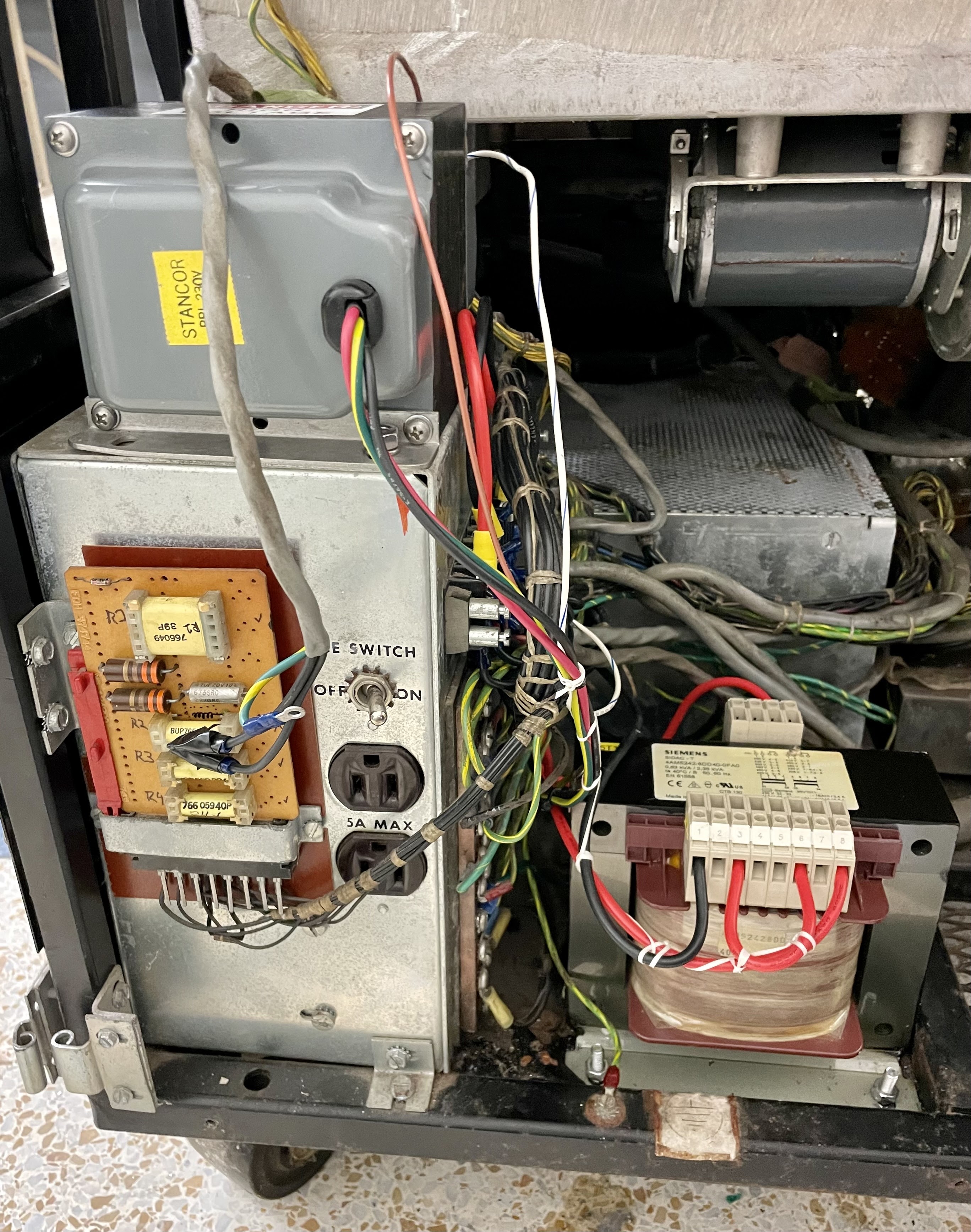 |
| T3 in lower right and T2 upper left |
TEDIOUS WORK FINDING CONNECTIONS ON THE CARD
Since there are 21 rows of 26 columns on the double size SLT card, the number of combinations to test in order to discover every connection is massive and infeasible to perform blindly. The situation is slightly better than it appears - not a combination of 2 items from 556 possible points - due to some points we can exclude.
The first row is used to mount the power rail filter capacitors and to carry some card pin signals over to the opposite side of the card, thus we can ignore those 26. Each of the SLT modules has four pins in the center which are used to connect the power rails and ground, so they can be excluded as well. This gives us 96 more points to ignore.
Therefore we are looking for the number of combinations of two points selected from the 424 possible signal points. There are 'only' 89,676 blind tests to perform. That number can be further reduced by awareness of unused pins on specific SLT modules, and by excluding some open spaces between the SLIT modules when there is no other component mounted.
That might get us down below the 50,000 neighborhood of tests. At 3 seconds per test, that would require around 42 hours of continuous work. I don't think I could work at that pace anyhow, but this is well into the impractical tedium zone.
MAPPED OUT ALL THE RC MODULES USED ON MY CARD
I did manage to finish mapping all the components - with a bit of ambiguity that remains because a) in-circuit testing can produce invalid measurements due to effects of connected components and b) a pair of pins may be connected on the SLT card but not actually connected in the module.
MAKING USE OF MY BREADBOARD SYSTEM TO HANDLE SLT 3V SIGNALS
I have an E&I CADET breadboard system which has some very convenient features for working with SLT. In addition to a standard TTL +5V power rail, it has variable positive and negative power rails which I can use to generate 3V for compatibility with SLT.
It also lets me set up the logic switches and the signal display LEDs to operate with either +5V or my variable (3V) supply level, so I can use these to create inputs and show outputs without building any interface circuits.
BUILDING MORE BANANA PLUG TO BREADBOARD JUMPERS
A double SLT card has 48 pins but 8 of those are standard power connections (and for this particular card there is an additional pin used to increase current capacity for the +3V rail). Four pins are not used on this card, thus we are left with 35 input or output pins that I have to connect to test properly.
I will the using the breadboard to source and sink the connections, either setting inputs to static levels or using switches, while displaying the outputs. To make this work, I need jumper cables with a 22 gauge wire on one end and a 4mm banana plug on the other.
The process of creating them involves, removing the covers, cutting and stripping wires, soldering wire to the plug, then reinstalling the covers - repeated for each jumper. I have 29 jumpers completed and have already cut and stripped the wire for the final 11 I intend to build.
I also purchased more stackable colored banana plug to banana plug jumpers, since I need a pair for each voltage rail at a minimum plus the ground wires running to and between supplies.
SET UP TO PRODUCE THE ALTERNATING CLOCK INPUTS TO DRIVE THE SLT CARD
The clock inputs to the SLT card I am troubleshooting must be a pair of signals of alternating phase, not just a single ended clock. I chose to produce that by setting up a 74ALS05 and a 74ALS35 chip on the breadboard. These are inverting and noninverting hex gate DIP chips that are pretty ideal to feed a square wave and get out a pair of out of phase signals to send over to the SLT card. Being open collector chips, they are magically 3V SLT compatible even though the chips themselves operate on 5V.
 |
| Breadboard with twinned hex gates for clock signal |
My breadboard system can generate a square wave up to around 100KHz, not as fast as the clock in the 1130 but suitable for initial debugging of the card. I can switch over to my function generator that will produce a true 2.25MHz square wave for full speed verification.
No comments:
Post a Comment