WORKSHEET SO FAR
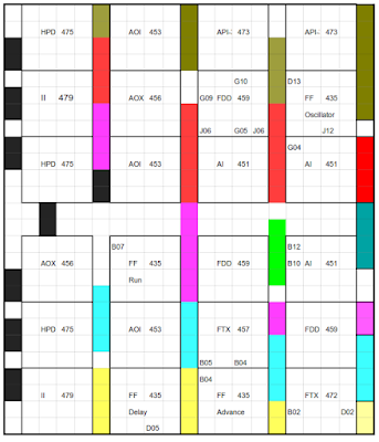
The grid has one box for each of the potential holes in the board where components mount - in real life they are .125" apart, a bit larger on this image. An SLT module fits on a 4x4 space, which I mark with thin borders. There are 12 signal pins around the perimeter and the center block of four are the power/ground pins
I also marked the type of module and the last digits of the module code. A flipflop (MGTR) is 361435 for example. With the flipflops, I wrote the name that they have on the ALD page.
The two single shots are implemented by the FDD and FTX modules on the right column, bottom two rows. The outputs are on pins 2 and 9, where I wrote the card connector pin B02 and D02 that are wired to these points. The Delay flipflop has a connection to card pin D05 where signal -Delay is output.
I haven't finished marking all the inputs and outputs yet, but this is a documentation method I will make use of for my overall work with the card. I can then make versions of this with the connections marked that complete some gate or set of gates where I am debugging.
As an example, the single shot involves half an FTX, half an FDD, plus some resistor packs, a capacitor and an inductor. The input pin to the single shot would be shown going to the output of some interior gate on the card which drives the SS.
No comments:
Post a Comment