Friday, December 12, 2014

Some coding and design work done while traveling to and from Shanghai

Long silence from me - thanks to the Great Firewall of China, which kept me from Facebook, Google, Youtube and most blog sites while I was in Shanghai. On my last flight leg coming back now, Thursday evening. No more trips for the time being - finally back to the 1130.

SAC INTERFACE FOR ADDING PERIPHERALS TO THE 1130

I made quite a bit of progress on the SAC interface logic, coding up VHDL to support up to 20 peripherals, whether fully physical or partially implemented in a PC. The link basics are built, allowing the PC to service devices. In addition, I created a special pseudo device which can load or dump memory contents from the 1130 as well as providing diagnostic support  by watching memory locations and some status conditions.

I worked out the basic skeleton of the access to the link from the PC, using the Digilent Adept SDK to find and use the USB based connections to my fpga board. The library is built as C DLLs but I wanted to write my PC code in Python, which involves a bit of adaption with the ctypes module and others inside python that allow me to call C libraries and manage their expected data types.

Without the hardware, my testing was limited, but I was able to build up my skill with ctypes and Adept so that I should be able to move reasonably quickly after I get home.


Sunday, December 7, 2014

Wiring up power supply of the SAC Interface box

SAC INTERFACE FOR ADDING PERIPHERALS TO THE 1130

I ran the circuit simulations with the 5V supply to my circuits reduced to 3.3V, to simplify the link to the FPGA board which is easiest to operate with 3.3V logic levels. Everything worked well, thus I will drop the use of +5V for my logic levels and instead use 3.3V for the FPGA side and regulate the 5V source down to +3V for the SLT side.

Heat shrink over solder joints, connectors now in place
Filter capacitor for 3.3V FPGA side supply
Filter capacitor for 3V SLT side supply
I installed the filter capacitors and wired up all of the power lines except for the 3V voltage regulator which is on-order. I set up a barrier strip to wire in the regulator, allowing me to set up all the other wires. There are just a few remaining tasks before I test and then begin using the SAC Interface box:

  • Wire the case fan to the 12V and ground lines
  • Finish the mounting brackets for the 26 pin power connector
  • Install the 26 pin female connector that brings the 1130 power and EPO lines to the box
  • Build and install the 3V voltage regulator
  • Secure the 24V relay inside the case
  • Hook up the front USB port cable to the FPGA's UART micro USB connector
  • Connect the second front panel USB port to the FPGA programming micro USB connector
Nearly complete now - just a few tasks remaining

Power supply and wiring work on SAC Interface Box

Working at a conference in Las Vegas this week - non stop giving talks, meeting with attendees and other activities from breakfast to dinner time. I was only able to snatch one or two tiny intervals when I had breaks and needed the change of pace. Not much was done but now that I am back home, I could pick up the pace. I didn't post this until Sunday morning but it represents the day's work yesterday.

SAC INTERFACE FOR ADDING PERIPHERALS TO THE 1130

I began setting up the Python environment and getting things in order to code the PC side software for the interface link. This includes the ctypes library that helps with calls to C based libraries such as the Adept2 from Digilent.

My naive assignment of signals to pins on the breakout board assumed that each pair of FPGA inputs (e.g. LA01P and LA01N) were assigned sequentially, beginning with LA00P at pin 1 and ending with LA19N at pin 40. When I looked closer, that wasn't a valid assumption. Instead, the pairs are assigned in the pattern LA00P at 1 and LA00N at 3. LA10P is at 2 and LA10N is at 4. In other words, the pairs are not wired vertically to each column of the two-row connector. The bottom row has the pairs assigned left to right, then the top row continues with the next ten pairs, assigned left to right.

My SAC interface cards are wired into the connectors in the pattern I expected, so that a register might be assigned to pins 1 through 16 sequentially. I worked out all the FPGA signals that correspond to the breakout board pins, which allowed me to map the fpga inputs to the proper logical signals in the hop-around pattern the board actually takes. It was time consuming but now all is correct as far as I can tell.

Twisted pairs to interface board stack from right, single ended lines to FPGA board at left.
All the wiring of the interfaces to the fpga board connectors is done and I am finishing the insulation of the 'joins' where I soldered the stranded wire that fits crimp connector pins to the solid wire that is easy to insert into PCB board holes. I used heat shrink and my hot air rework gun to insulate all those ends, then wrapped groups together with electrical tape.

Heat shrink insulation of solder joints on wiring to the connector
An ATX power supply fits into the case and serves as a good source of 12V, 5V and 3.3V power for my unit. I used a 24VAC relay for the 'power' switch of the supply, which will connect to the 24VAC power that is used in the 1130 system to power up all peripherals. I still have to add filter capacitors and a voltage regulator to get the 5V and 3.3V sources to the exact levels of 5V and 3V that I need. The FPGA board takes a 12VDC input, directly from the ATX supply so it will come up as the 1130 itself is turned on.

ATX power supply in place and 24VAC relay loose on top for remote power-on by 1130

1442 CARD READER/PUNCH RESTORATION

I spent a bit of time cleaning and inspecting the parts from the feed clutch that I had disassembled before my trips, in anticipation of re-installation, lubrication and adjustment. I didn't begin the assembly itself today but expect to get to this (plus finish the 1053 console printer repair) soon. 

Sunday, November 30, 2014

Installed new drive belt on 1053 console printer

1053 CONSOLE PRINTER RESTORATION

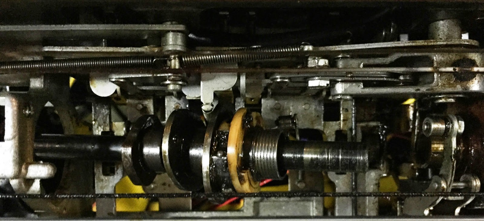
Due to the rain, spent time inside the garage working on disassembly of the cycle shaft in order to replace the motor drive belt on the console printer. By 9:30 AM I had the new belt in place, with the cycle shaft hanging loose in the frame. Reassembly should not be not much harder, but then comes all the adjustments that now must be made since I had to disturb so many settings with the removal.
Removing various parts in order to move the cycle clutch shaft
Cycle Clutch shaft pulled to left, allowing access for new belt

The pulley in the middle is where the drive belt is installed
New drive belt installed but shaft not yet reassembled
By mid afternoon it was reassembled but not yet adjusted. Later I have to adjust:

  • backlash on gears
  • lateral play on cycle clutch latch (should not have changed)
  • cycle clutch latch height (although I didn't unfasten it)
  • cycle clutch spring angular position (timing of clutch release)
  • filter shaft timing relative to cycle clutch shaft
  • print shaft timing relative to cycle clutch shaft
  • C2 contact timing (feedback to 1131 while the print mechanism is busy)
I am off early tomorrow morning on a trip to Las Vegas, returning Friday evening and will be celebrating my wife's birthday tonight as I will be out of town on the actual birthday. No more work on the physical system until Saturday but I will haul along the tools to continue writing code for the FPGA and for the PC side software, in any free moments I will have. I don't expect many as I am fully booked for the entire conference.


SAC INTERFACE FOR ADDING PERIPHERALS TO THE 1130

Lots of rain today, no chance to set up outside and continue with the wiring.

Saturday, November 29, 2014

Beginning console printer disassembly plus more wiring of the SAC Interface Box

Two impediments to working today - heavy rains and a road trip to visit a dog we might adopt. I did what I could inside the garage, turning to some mechanical rehabilitation that was reasonable while shut in.

Due to congestion in the garage, wiring and construction projects are easiest to do by setting up a long folding table just outside the front of the garage, with the door raised, but that won't be much possible with the heavy rain underway.

Instead, I will drive over two hours each way to meet with an owner of a dog my wife is considering adopting. Our family dog passed away a bit over a year ago and she feels it is time for another one to live with us. Back in the mid afternoon, I could then move into the garage for an abbreviated work day.
Kerry, the dog we hope to adopt
1053 CONSOLE PRINTER RESTORATION

I forced myself to sit through the entire video series (Selectric Training) on Youtube, hours long, to be sure I was ready to tackle the replacement of the drive belt on my 1053 console printer. The course was released as audio cassettes plus color slides, which someone has now combined into a series of videos and uploaded. The narrator speaks slowly, which gives the entire course a plodding feel, dragging along but with short bits of important information sprinkled throughout.

I took off the front panel and cover of the console printer and prepared to disassemble the cycle shaft. The first couple of steps involved removing the cover over the gear and taking off the degree wheel that rotates at the left side of that shaft.

Covers and front panel removed, ready to start surgery

The cycle shaft is the left 2/3 of the picture

SAC INTERFACE FOR ADDING PERIPHERALS TO THE 1130

The skies cleared up late in the afternoon allowing me to set up the table outside and get more completed on the interface box. I have the hybrid solid/stranded wires with the crimp pins installed for all the signals and have installed the 12 driver signals from board three into the fpga connector.

I accidentally installed two pins out of order but I will correct this by breaking the joint and swapping the stranded wires to the opposite solid wire. In this way, I don't have to extract the pins from the connector to move them to another spot. They stay in place but are hooked to a different wire to the interface board. There was no more daylight at this point so I had to stop the work.

I have five more driver pins to install into connectors, those hooked to board four. As well, I have the 12 receiver pins from board three to install before this wiring is complete.

Friday, November 28, 2014

More construction of SAC interface box

SAC INTERFACE FOR ADDING PERIPHERALS TO THE 1130

I got up and began working as soon as the sun was up enough to light my worktable in the garage, my top priority being to finish the interface board wiring to the 160 pin socket and to the connectors that will fit onto the fpga board assembly.

I found that the rigors of pushing in the pins to the connectors would often stress the solid wires I had used for the links, I decided I had to abandon those and replace them with thin stranded wires. I hate connectors,  which often become the most fragile part of my assemblies.

In this case, my decision to insert wires directly into a circuit board on one end and into crimp on pins for the other left me with a 'no win' scenario. Pushing multistrand wire through a PC board hole is an exercise in frustration, but using single conductor wire to the crimp connectors inevitably leads to the wire snapping off the connector after some degree of flexing.

The leads from the 160 pin socket to the board have the same issue, but one I optimized for ruggedness by using stranded wire on that side. I soldered a small section of solid wire to the end of one side to form a 'pin' I could push into a PCB hole and solder.

I will need to replace all the TTL signal wires with stranded wire, solder on solid 'pins' for the PCB side and crimp them on at the connector end. I realized I can use the ends of the existing solid wire, where they exit the PCB, as the 'pin' to avoid having to rework three boards times 24 leads each plus another five on the last board. Unsoldering, cleaning up and resoldering all that would have been a major pain.

Another task for the day was to select the mounting location for the FPGA board stack, drill the holes and mount it inside my enclosure. I made a paper guide for marking and drilling the bottom of the cabinet. The stack of two boards, FPGA and debugging/breakout,  is now mounted in place and ready for the connectors to be affixed.

FPGA board and breakout daughter card mounted inside enclosure
By 4PM, after working most of the day, I had the TTL side signal wires from the first two boards attached to the connectors and had begun on the third board. When the rest are hooked to the connectors, I have to tape up the soldered junctions between solid and stranded wires, dress everything up with cable ties, and then install the connectors onto the breakout board.

Separating interface boards while wiring them to fpga connectors
There is too much to do in the remaining daylight, so I will move inside and work on coding. I am implementing the FPGA side basic link to communicate with a PC (and also have to write the software to run on a PC.) The Visual Studio support for Python looks solid and I should have no problems using accessing the Adept libraries by using the 'ctypes' package in Python.

Thursday, November 27, 2014

Completed SAC Interface 1130 side IO capability, working on PC side

I completed more logic definition during the long flight from London to Los Angeles and on the ground switching flights, but didn't arrive home until the evening. As a consequence, I didn't do any construction or hands on work in the garage that day and today is Thanksgiving so I only got out for a few minutes today.

SAC INTERFACE FOR ADDING PERIPHERALS TO THE 1130

I completed the functionality to support up to 20 devices with the SAC interface, each configurable on the following dimensions:
  • area code (device address)
  • XIO functions supported
  • Use of cycle steal
  • Interrupt level(s) used
  • Priority of devices for cycle stealing
I am building some black box modules that the synthesis tool will assume are producing real input signals and/or are consuming some of the signals I generate. If I didn't do this, the synthesizer would recognize when outputs weren't used, trimming away all the logic to create them, Similarly, if there is no input or it is a fixed value, logic is trimmed away or replaced by a constant output. 

Careful attention to the synthesis report and all its fussy warnings is a best practice for successful designs, as these warnings may show a flaw in the logic or a missing connection. Even when it is purely noise, a bit of modification to the source can remove most of them. In that way, any warnings that do arise as you make changes have a reasonable chance of flagging real issues. 

I did some work on the link to a PC, which provides data, control and status for an emulated peripheral, but still have some design decisions to make before it can be fully implemented. 
It will leverage the Digilent provided USB system using the async parallel port mode, a quick way to allow code on the PC to send or receive data from a pool of up to 256 one byte 'registers' which are whatever signals I need. These will be the data out and in buffers, plus status and control information, for each of the implemented peripherals.

The logic to transfer pairs of registers (16 bit entities to match the 1130 architecture) is in place in my VHDL, ready to be used for functions inside the interface. The first two I will implement are a cycle steal access to memory and a display/update of SAC interface signals.

To create the PC side code, I set up Visual Studio Community, the free version of VS. I will use Python for my code unless I find some technical impediment to using the Digilent Adept software with that language.

I received the FMC Carrier S6 FPGA board, the Xilinx breakout board that attaches to it, and the parts for the plugs to connect my signals to the breakout board. In addition, I picked up a set of HP standalone probes - a logic probe, a logic pulse injector, and a current probe - that will be handy to identify which of the many drivers of a wired bus is driving the output to 1.