INSTANTIATING A MODULE WITH THE SAME INPUT OUTPUT BUT MINIMAL LOGIC
I took the interface design of the memory controller module and used that to build a false memory module. It was easy to stick that into my design, although I did have to drive a few signals and provide the clock that the rest of the system depends upon.
A clock module was built into the fake memory module to provide the 50MHz main clock for my FPGA logic and I forced the app_rdy signal high to indicate that the controller is ready for commands. I then worked up a delayed response to signal that the data was available from the RAM read, sending the data valid signal four cycles later to ensure that my driving logic is sound.
SPEEDUP IN SIMULATION SPEED, MORE THAN 10X FASTER
My VHDL is simulating much more rapidly now that it isn't trying to represent all the gates inside a memory controller. I believe it is at least ten times faster, perhaps as much as 15 times faster, which makes a simulation run bearable as I iterate testing and repairing my logic.
WORKING MY WAY THROUGH THE READ REQUESTS UP TO THE RAM MODULE
The high level flow of my logic is that as we begin on the next word being read in a sector, we push a 48 bit request that contains the address in the RAM and a bit that requests a read (16 bits are unused for reads but contain new data on a write).
The FIFO that has had the request inserted alerts the FIFO emptying process to pull the request, which then triggers the RAM engine. I correctly set up the addresses, the read command byte and the enable flag for the two cycles needed to cause the memory controller to begin a read. Several cycles later the RAM has completed the read and turns on the ram_done flag.
At this point, the response FIFO filling process would package up the word just returned and push it into the queue. The FIFO emptying process will load that content into the active word register which is used to shift out the 16 bit cells plus the four check bit cells.
I verified up to the activation of ram_done at the proper point. Tomorrow I will watch the response FIFO work and check to see whether the new word is in place fast enough for the generation of the first bit cell.
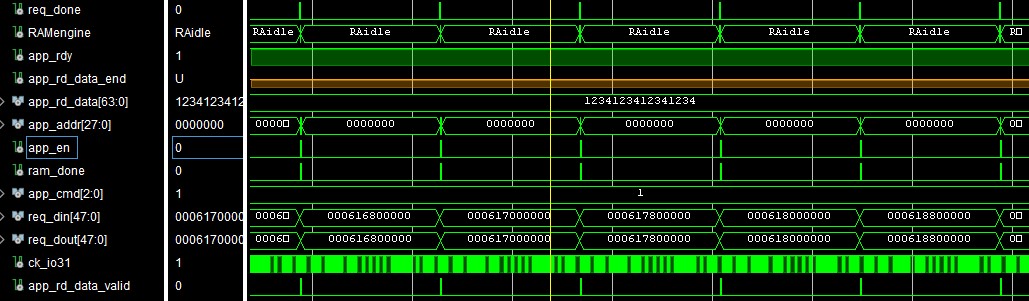 |
| Triggering the RAM engine to read each word |
Hi Carl, It's probably of no impact on the project, but DISKN "minimizes extra disk revolutions in transferring more than 320 words." I know you are working much lower than this, but I don't know how DISKN achieves faster write time time. When you get to the point of testing with DMV2, you might want to try DISKN to see if it gives your interface any trouble. Thanks for all your hard work. Bob.
ReplyDeleteThe alternative to diskn is to issue separate disk calls - each then involves waiting until the sector comes around. Due to delays with the interrupt and other software before the new IO starts, that often means most of a rotation, up to 40ms, is wasted.
DeleteDiskn issues multiple read XIOs bearing in mind where the disk head will be which would minimize rotational delay.
It doesn't do anything other than XIO Init Read or XIO Init Write to a sector at a time, so the results should be identical. I model the exact timing of a rotation - the delays or lessened delays should be identical within the accuracy of the real rotation rate of a physical drive versus the 'perfect' RPM of my circuit.
Still, good thing to test, notes taken.