IBM 1130 PROVIDES SIGNALS FOR DEVICE CONTROLLER CIRCUITS
There is logic in the machine to decode the 'area' in an input-output request. It turns on a signal for each installed device that the designer of that device's controller can test to know when I/O is being directed at the device.
The XIO (Execute I/O) instruction points at a doubleword in memory called an Input-Output Control Command (IOCC). Among the fields in the IOCC are a five bit area that identifies a particular device and a three bit command type. The keyboard is area 00001 which distinguishes it from other devices such as the 1442 card read (00010) or the internal disk drive (00100).
There are six possible command types but each device determines which of the six are used with it. The keyboard supports just three commands, B'100 - Control, B'011 Sense Interrupt and B'010 - Read. The Control command causes the keyboard to be selected. A solenoid in the keyboard should unlock it and the Select KB light on the console near the keyboard should illuminate.
When the operator presses a key on a selected keyboard, it triggers an interrupt on level 4. IBM 1130 interrupts are prioritized, levels 0 to 5 and each device is assigned specific bits in one or more interrupt levels.
This means that when the interrupt occurs for level 4, the interrupt handler that is executed has to call the device driver code for the keyboard when its sees the bits for that device are set. The interrupt handler issues the XIO command Sense Interrupt to put the bits of the status word in the Accumulator. One of the bits in level 4 tells us that a key was pressed on the keyboard.
When we know that a key was pressed, the device driver should issue an XIO with the Read command, which picks up the code for that keypress and puts it in the memory location we specify in the IOCC.
The device controller, which is implemented on a number of SLT cards in the machine, will handle a read command and put the value of the keypress on the B register so that the XIO in its storage cycle E3 will store that B register into the memory location.
The device controller is connected to three signals - XIO Read, XIO Control and Area 1. When it sees its address (Area 1) is active, if XIO Control is active then it triggers the solenoid and turns on the select lamp. If area 1 is active and it sees XIO Read, it puts the keypress data on the B register. There is a bit more to the device driver but it is relatively straightforward.
 |
| Selecting the keyboard with a Control command |
I watched the Area 1, XIO Read and XIO Control lines to see if they activated as I stepped through an XIO instruction with the appropriate IOCC. If I didn't see these, the problem would lie in the general logic that supports all IO devices. If these did occur, then I would need to move forward in the device controller to see why it is not selecting the keyboard and doing the other actions.
OBSERVATIONS TESTING THE XIO CONTROL TO THE KEYBOARD
When I observed the first signals I could clearly see Area 1 turn on when an XIO was addressing the keyboard. What I did not see was XIO Control activating. That signal is produced at the correct time during an XIO instruction when the command is a control, in other words when bits 5, 6 and 7 are B'100. There is some simple combinatorial logic to determine this.
 |
| Excerpt of logic that generates +XIO Control |
Looking at the inputs to the AND gate I found that the signal -U Bit 7 was not high. The other conditions were all true but not this one. It is driven by an inverter gate and I soon found that the input to the inverter was not actively driven high or low.
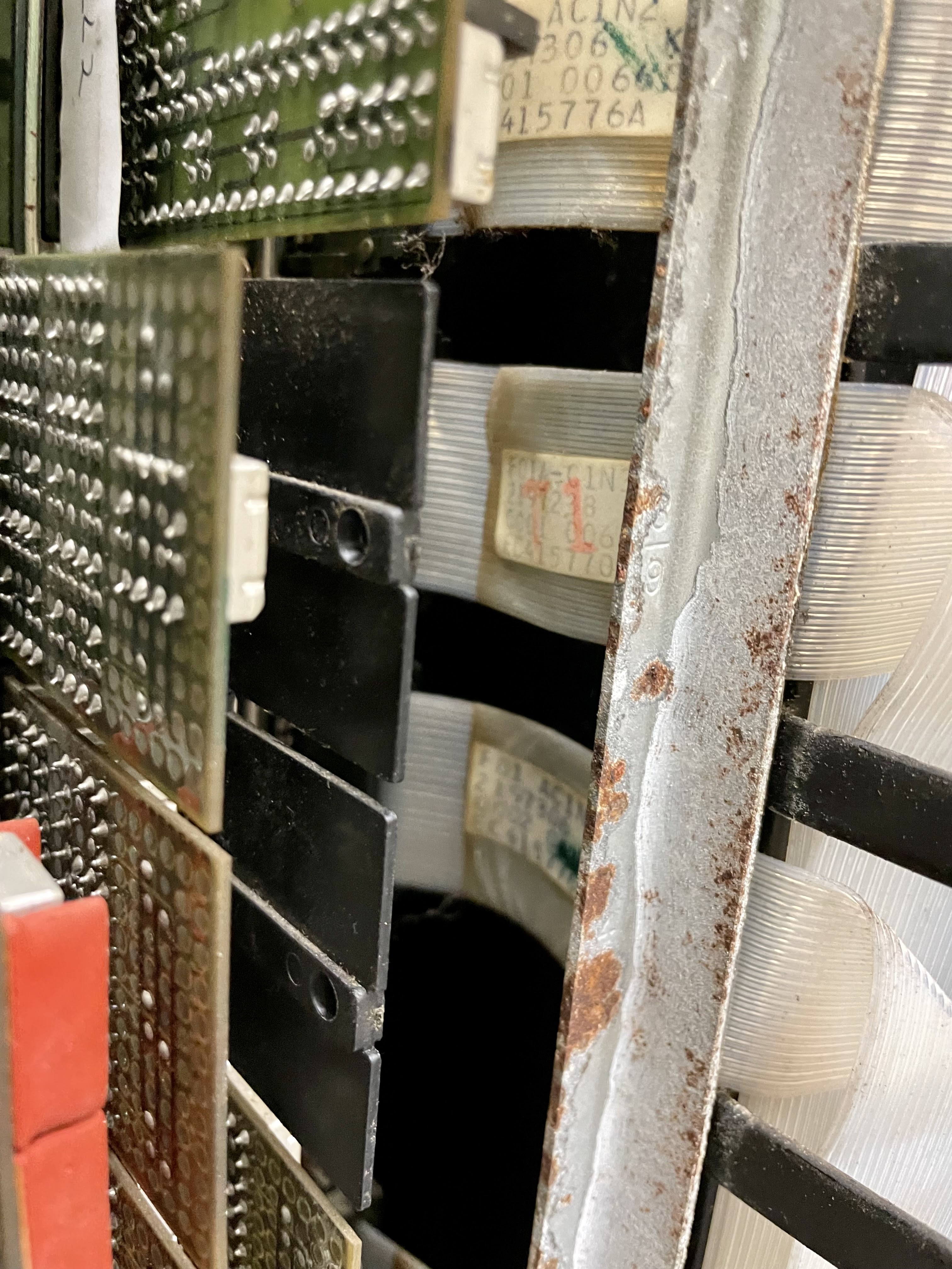
This signal comes from B gate over to compartment C1 of A gate where this test is made. The signal enters A-C1 from edge connector N3 on pin D05. The other end of the cable plugs into the bottom of the backplane at B-B1 in slot T5 with the signal emerging on pin C04. I verified that the signal does indeed span from T5 pin C04 all the way to the inverter using the signal in A-C1 compartment.
 |
| Source of signal in B gate B1 compartment |
What failed was the routing from the SLT card generating the signal down to T5 pin C04. Another bad trace on a backplane from an edge connector to the interior of the backplane. I put in a temporary jumper and now the KB Sel lamp lights when I issue the Control command to the keyboard, just as it should.
 |
| Control command now activates keyboard |
 |
| Temporary jumper |
The prior backplane trace to edge connector was on the backplane A-C1 on the left edge. This trace failure is on backplane B-B1 at the bottom edge. More than one event or failure has occurred here, nothing in common.
 |
| Edge connector cables entering card compartment |
I am getting worried about further failures of traces. Two backplanes out of six have at least one trace failure. The only experience I had during the restoration of my own system was with a trace failure that broke the ground rail to part of a core memory backplane. Once I fixed that, I never had another problem on my system.
Therefore, it is possible that I just happened to find the two problems, if that is all that exist, but I will need to do extensive, exhaustive testing of every function and every permutation and corner case to be sure that key signals aren't missing elsewhere. There are quite a few cables between backplanes.
 |
| Map of cables between backplanes and other locations |
I will correct these more permanently with wire wrap connections, removing the jumpers.
PARITY ERROR ISSUE IS ALWAYS CAUSED BY BIT 0 FLIPPING FROM 0 TO 1
After some experimenting I realized that when I get a parity error it is always a case where bit 0, the leftmost bit in a word, had been a 0 but becomes a 1. This causes a parity error reading it since the parity bit was generated for the intended value of 0. Once it flips it remains a 1.
This is not an error reading out the bit during destructive reading, since the error would go away on the next attempt to read it. The intended data value was 0 for that bit because the parity is generated for that case, but somehow the inhibit wire is not blocking the bit flipping on during the write part of the storage cycle.
The way that core storage is designed is to select the X and Y rows for a given address, which would flip the bit to a 1 because the currents in X and Y combine to be large enough to flip the magnetization. If a current is sent down the inhibit wire in the opposite direction, it neutralizes some of that magnetic force and blocks the core from flipping.
What we know is that the sum of X, Y and the reverse inhibit are strong enough to flip the bit whether inhibit is on or not. Most likely it is an issue with the inhibit driver or some setting, affecting only bit 0. I will have to do some scope tracing to figure out what is behind this issue and correct it.
I BEGAN DEOXIDIZING THE CONTACTS IN THE KEYBOARD
The keyboard of an IBM 1130 is the keyboard from inside an 029 keypunch, with a few different labels on keycaps. The encoding of a keypress is Hollerith code, as a consequence. The IBM 1130 peripherals do not translate their characters to a common encoding; each device has its own coding, forcing the programmer to make conversions. A letter on the keyboard comes out as Hollerith. Typing that on the console printer requires the issuance of the shift and rotate code of a Selectric typewriter (in the PTTC/8 rather than typewriter encoding). The programmer must do a table conversion of what is typed in to print it out.
The keyboard is mainly mechanical in its encoding. Each keylever selects a combination of movable vanes on the rear of the keyboard. These open or close contacts on the side. In addition, thin metal bands below the keystem have contacts that can reshuffle the output of those contacts on the side. One final set of connections is altered when the Numeric key is held down, since one keycap can represent different characters when shifted.
 |
| 029 Keypunch keyboard repurposed as 1130 keyboard |
 |
| Side contacts controlled by permutation mechanism |
 |
| Numeric and keyboard restore buttons |
 |
| Keypress detection switch |
 |
| Key stem activation contacts |
There are some electrical contacts in addition to the encoding role above - for example there is a microswitch for the Rest KB button that will restore the keyboard, removing any pressed keystroke.
The normal process for the keyboard is that a solenoid will reset the keys, thus 'unlocking' the keyboard. Any key that is pressed down will lock the encoding (permutation) mechanism and leave the key down. No other key can be pressed. A switch detects that a key is locked down and triggers an interrupt so that software can read the encoded value of the key. The act of reading the value also resets the KB Sel lamp.
The software that manages the keyboard would typically immediately issue another Control command to select the keyboard to allow a next character to be pressed, as long as it is looking for input characters. Each Control command fires the solenoid to reset the keyboard so that it is ready for the next keypress.
The contacts in the keyboard mechanism are prone to oxidation. I used a cleaner plus a burnishing tool, a thin blade just round enough to scrape off a thin layer of oxide without damaging the underlying metal. When I return to this task, I will use the continuity tester to verify good contacts and proper encoding.
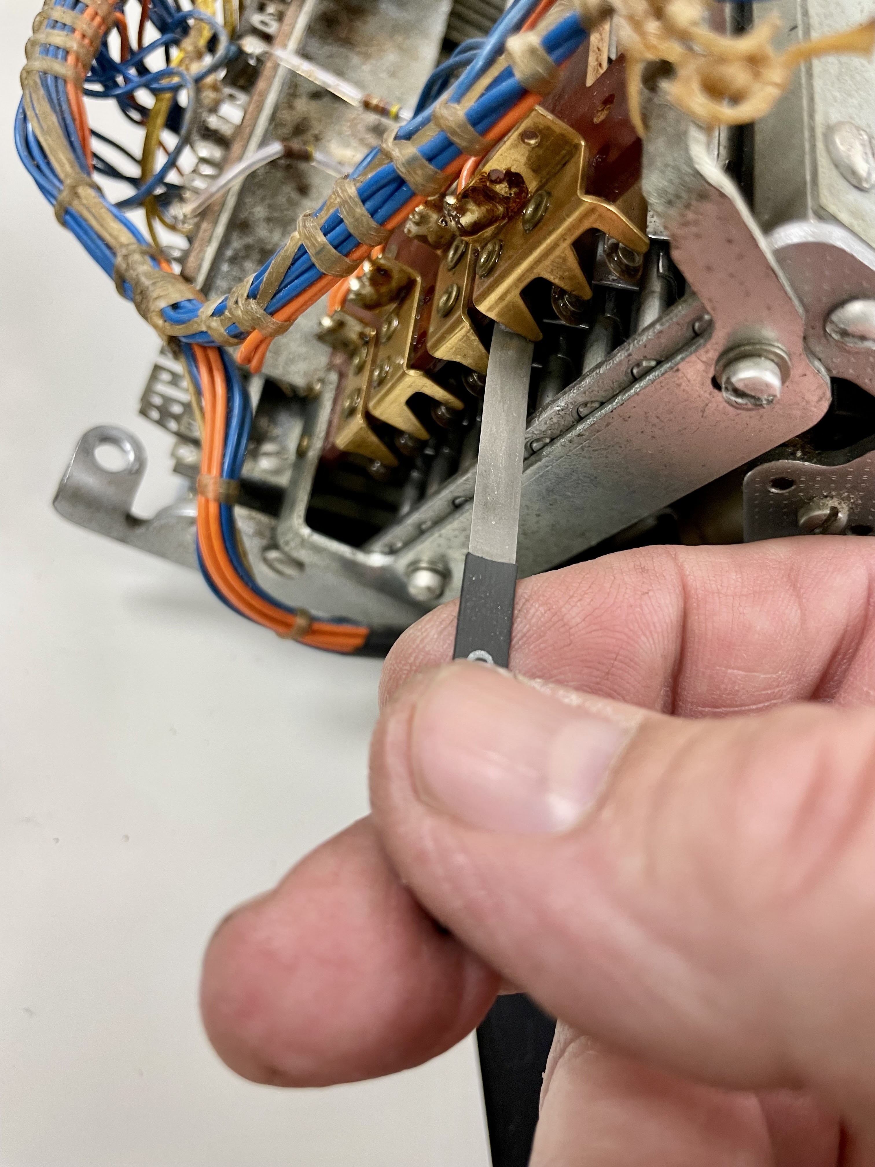 |
| Burnishing contacts |
LOCATION FOUND FOR THREE RELAY BOARDS TO ADD MEMORY LOADING TOOL
Hand entering instructions and data is a slow process, involving flipping the sixteen console entry toggle switches, pushing the Prog Start button and sometime loading new addresses and hitting the Load IAR button. To make entry of code more palatable, I designed a simple mechanism around some relay boards and an Arduino that will activate the console entry switches and virtually push the Prog Start and the Load IAR buttons.
It has a very simple protocol that takes lines of four hex characters plus an initial code when this is an address rather than contents to be loaded. A program on a PC would talk to the Arduino over the USB cable and transmit long sequences of words to be toggled into core memory.
This will be very helpful in debugging the machine, where portions of diagnostic programs can be loaded and run. Normally this would be done with multiple boxes of punched cards through the card reader or reading the programs from a disk cartridge, but this system has no reader and the disk drive is not yet working.
While I designed the tool for The National Museum of Computing in the UK for use with their IBM 1130, I hadn't needed it on my system. TNMoC decided where to locate the relays and other parts, not me.
The reason I didn't need it is an optional feature on my 1130 called the Storage Access Channel (SAC) that I connected to an FPGA based box that lets me directly write and read memory using a DMA-like function called cycle steal. This is much faster and more direct than toggling in code with entry switches and buttons, but neither the machine at TNMoC nor the one I am currently restoring have a SAC.
Since I will install this tool, I have to make design choices for installation and wiring. I found a nice location under the table top, just behind the keyboard, where the relays can be mounted on drilled holes and neat wiring can connect them to the Prog Start button, Load IAR button, +12V supply, 16 console entry switches, and ground. Small cables will connect these to an Arduino and a power supply in a small project box placed near the CE switches inside the top cover.
No comments:
Post a Comment