SPENT A COUPLE OF HOURS CHECKING CONNECTIVITY AND EXAMINING OPERATION
Two identical current control cards, one in B2 for the Y wires and one in M2 for the X wires. Swapping the two cards does not move the problem it remains on the X wires. The X wires show current during the write(back) part of the memory cycle, just not during the read portion.
Since the two cards receive almost the same signals and all the same voltages and other sources, I checked connectivity pin for pin for M2. Everything runs where it should.
THINKING ABOUT WHERE THE PROBLEM COULD ARISE
The problem occurs for any addresses, everywhere in the entire 8K of memory. Lots of things that cannot be the cause, due to this fact, such as:
- X wire breaks, since this occurs on all X wires
- Steering diodes, again since it affects all addresses
- Read gate and read driver cards since there are many across the address range
- Timing control signals, which are verified to be correct
- Failure of traces on the backplane - I have checked out every one to card at M2
A connection is made across one wire by the Read Gate selecting a group of signals and the Read Driver selecting an orthogonal set of signals, isolated by steering diodes. Many different gate/driver cards are involved and none connect the path. This suggests that the issue is in the current sink. A read involves the Read Gate delivering the +8.3V to one side of the X wire and the Read Driver connecting the steering diode output to the current control card in M2 which sinks a controlled amount of current.
The pseudo-schematic provided by IBM is quite complex to parse, thus I broke down the diagram to just the portions involved in a read operation. Here is the original IBM diagram below.
This includes all the circuitry for both read and write, as well as the four parts that generate an internal 1.4V source used in various parts of the circuit.
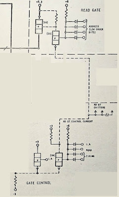
Starting with the Read Gate circuit, the purpose of which is to connect +8.3V to one end of the X axis wires, I extracted and simplified to the following diagram:
The address bits 6, 7 and 8 are connected to the top set of diodes, which selects and activates only the circuit for that particular combination of bits, e.g one for 010, another for 100, etc. That turns on the upper right transistor, but nothing happens until the bottom section is activated. The lower right set of diodes get the timing signals such as +Read Cycle, to turn on the lower right transistor.
That action switches the emitters of the upper right transistor and all its peers on other Read Gate circuits, from +3 when idle to -3V when the bottom control activates.When that upper right emitter is pulled down to -3V, it switches on the upper left transistor to deliver the +8.3V to the X wire.
We also need the Read Driver circuit, which I have extracted and simplified below (but with a missing -3V on the bottom left):
The diodes in the upper left are connected to address bits 3, 4 and 5 and the circuit shown is wired to one specific combination of those three bits. This turns on the two transistors in the mid left. One connects the far end of the X wire to the current sink circuits on the lower right. That transistor can only be turned on if the one to its left is turned on. That in turn needs its emitter to be pulled down to -3V from +3V similarly to how the gate side circuits operate.
When the timing signals, e.g +Read Cycle, are active for a read, the lower left transistor pulls the emitters of the upper transistor down to -3V. The mid left transistor is turned on by the address bits in the upper left and pulls the base of the mid right transistor to switch it on. That passes the current from the X wire down to the current sink circuit on the bottom right.
The current sink circuit is designed to pull a target current level controlled by the Vref voltage. Adjusting V-ref adjusts the amount of current that will flow over an X or Y wire.
My conundrum is that the two current control cards have exactly the same V-ref and 8.3V connections. They are properly triggered by the correct timing signals. The address diodes on the top left of the driver and top right of the gate are used for both read and write; we see that current flows during write operations just not during read.


No comments:
Post a Comment