I captured the state of the Storage Buffer Register (SBR) after XIO Read of keypresses and those are correct even for the situations where we get the false parity check. The issue is after the SBR, in the circuits that set the parity bits and check the parity of the word about to be written back to memory.
DOESN'T MAKE SENSE THAT PARITY IS SET TO EVEN FOR SECOND HALFWORD
Each 8 bit half of an 1130 memory word is protected with an additional parity bit, which is set to make the total number of 1 values in those 9 bits be an odd value. In the case of the two keys I was pressing, F and G, the second 8 bits are either 10000000 or 01000000, both of which have an odd number of 1 bits and the parity bit is therefore set to 0.
The value actually written into memory is always correct, having odd parity, but the error detection circuit believes that the second halfword of memory has even parity, thus it latches a parity check and halts.
The parity is checked with a circuit which is a tree of XOR logic gates, culminating in a true value if the parity is even when checking all nine bits. The 3022 card implements those XOR gates plus a single inverter to supply the output with both positive and inverted versions of the parity result.
The first layer of gates take pairs of input bits, bit 8 & 9 to one XOR (a), bit 10 & 11 to another (b), bits 12 & 13 to a third XOR (c) and bits 14 & 15 to the fourth XOR (d). The outputs of the four XORs a, b, c and d are connected to two more XORs, with the a & b outputs fed to a gate (e) and the c & b outputs connected to XOR (f).
Those second level XOR outputs e & f are connected to an XOR gate (g) that produces the even or odd parity state of the original input bits. The output of gate g is combined with the parity bit value in XOR gate h, whose output is the parity state of all nine bits.
This tree of gates generates the +Even 2 signal when the second halfword parity is even. Based on the input values to the tree, its output should be false, but we see it only attain the false state for a short interval and then jump back to true.
SWAPPED PARITY CARDS AND THE FAILURE CHANGED!
Since the 1130 memory word is 16 bits, each halfword of memory is handled by a 3022 card. Slot K7 covers the first halfword, producing the signal +Even 1 while slot L7 covers the second halfword to yield +Even 2 where we are having our problem.
I swapped the two cards around and tested again. The results were quite different! Instead of experiencing a false parity error during the XIO Read instruction while it is writing the keyboard character code to memory, the machine generated a false parity error during the entry to the interrupt routine.
When an interrupt is requested, at the next instruction fetch time if no higher priority interrupt is active, the CPU will block core memory access and instead force in a value to the SBR. During the I1 cycle for this instruction fetch it forces in 4C40 during the write half of the memory cycle.
The next (I2) cycle fetches the second word of the instruction, which again is jammed in by the hardware while blocking core memory access. This is the value 000C which is where the location of the interrupt handler address is stored.
In the following IA cycle, core memory is allowed to operate and the machine fetches from 000C the address for our BSI instruction. The dummy instruction is a Branch and Store IAR, long format (double word) with indirect addressing. It finds the location of the interrupt handler and uses that to execute the function of the BSI.
A BSI stores the current IAR value in the effective address (target location), which was the address found in memory location 0000, sets the IAR to the effective address and bumps it by one to execute instructions starting at target + 1.
It is while the BSI has started an execute memory cycle for the effective address, wishing to save the IAR of the interrupted routine. It updates the SBR with the value of the IAR, using the -I to B SP signal which is very similar to the -I/O to B SP signal used for our XIO Read of the keyboard. Just as with the keyboard issues, sometimes the 3022 card generates a false even parity status leading to a parity stop.
Since the failure moved when the two cards changed places, this is definitive that at least part of the problem is due to different operation of the two supposedly identical card. This is presumptive for a defect on the card which was originally in L7 and was moved to K7.
Swapping the cards back restores normal operation of the interrupt entry but again exhibits the strange errors when sequentially pressed keys alternate across the groups I mentioned before, such as F to G or G to F. I looked forward to quickly finding the root cause and correcting it.
BENCH TEST OF CARDS FOUND NO DEFECT IN OPERATION
I set up my bench to operate the 3022 cards, looking to validate its generation of parity. I supplied the card with the standard rails of +3, -3 and +6V, a good ground, and then hooked up inputs and monitored outputs.
Both cards worked correctly and also identically. This was frustrating. The changing nature of the failure points to the card as defective, but I can't reproduce it on the bench. Due to other commitments there was only two hours to work on this today.
This is the schematic for the 3022 card:
LOOKED BENEATH AT THE ANALOG CIRCUIT, BENCH TEST NOT ACCURATE ENOUGH
I pulled up the schematics of the 3022 card that seems broken as well as the 3024 card that feeds the inputs of the 3022 card. IBM SLT gates are not standardized nor well behaved. The digital abstraction can be very different from the actual electrical behavior.
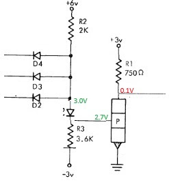
The typical SLT gate is the AOI (AND - OR - INVERT) which has diodes on the inputs so that current only flows out of the input of the gate to a lower voltage, usually ground. If the input is at or above the 3V point that the AOI gate maintains on the far side of the input diodes, then no current flows.
 |
| Basic AOI circuit |
This also means that a disconnected input is the same as a logic high input. In the simplified version of the AOI circuit below, the three inputs can be at 3V or floating, the result is the same. The junction to the right of the diodes is about at 3V and therefore the transistor is heavily conducting. That pulls the output pin to nearly zero.
 |
| No input at low voltage, thus output is low |
The defined logic levels for the medium speed version of SLT is 0V for low and 3V for high. Unlike modern logic families where a gate has a maximum voltage for a low input and a minimum voltage for a high input, all voltages in between being forbidden and avoided, SLT does not list these.
The only voltages listed other than the nominal 0 and 3V levels are 'transition point' voltages, which are arbitrary points on a rising or falling signal allowing the timing of the transition to be calculated. For medium speed SLT, one measures the timing between 0.3V and 1.8V for a signal whose extreme values are closer to 0 and 3.
The simplified version of the AOI shown below has one of the inputs connected to a voltage substantially lower than 3V. For convenience we will say this is 0V. This makes the junction to the right of the input diodes just a bit above 0 and the transistor base is essentially at 0V. It therefore is cut off, not conducting, allowing the pullup resistor on the right to make the output 3V.
Thus, SLT gates using diodes have only two logic states for any input - pulling enough current down to a lower voltage so that the transistor cuts off, or not. Those produce either logic high (3V) or logic low (0V) outputs respectively.
The consequence of this is that IBM is free to feed AOI gate style inputs with circuits that don't use a pullup resistor on the inverter transistor. The transistor is either conducting (pulling current to ground) or not conducting (effectively an open connection). Measuring these outputs is difficult because you won't see a voltage swing nor a clear indication of whether the output is logic high or logic low.
All of this digression was important to illustrate that these are not standard gates with well defined voltages. This is even more so with the parity circuits.
ACTUAL 3022 CIRCUIT WITH INPUTS DRIVEN FROM A 3024 INVERTER CARD
The logic diagram view is that inverters are delivering the SBR bits to the parity card XOR gates. Thus, when the corresponding bit value is 1 in the SBR, the inverter is at logic low and when the bit value of the SBR is 0, the inverter is at logic high. The XOR combines two of the bits from the SBR (through inverters) and generates an output that is logic high when the two inputs are different else logic low.
That is how I set up the bench test - delivering 3V to an input when logic high level and 0V when logic low. With those inputs the circuits performed as they should. No differences existed between the two 3022 cards.
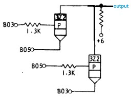
However, the inverters do not have pull up resistors, thus to produce a valid test the inputs to the 3022 should either be disconnected or grounded, not ever at 3V. Further, the 3022 card side does NOT use diodes as it true for an AOI gate. Here is the actual circuit, simplified to show just two bits from the SBR and a single XOR gate.
The XOR is unusual, so I will simplify the part of the circuit to the left of the inverter transistor:
However, if B05 is at ground but B03 is at 3V, the left transistor conducts and the right does not. This pulls the base of the inverter to zero. The pullup resistor then produces a logic high output because the bits are different. Similarly, if B03 is at ground and B05 at 3V, the right transistor conducts with the same outcome that the inverter produces an output of logic high.
This worked correctly on the testbench because I was supplying 3V or 0V for each input. This failed on the actual machine because the 3024 card does not supply a pull up resistor. That is a big problem because the XOR won't work properly.
HUNTING FOR THE PULLUP RESISTOR FOR THE 3024 CARD SBR BIT INVERTERS
The ALD shows me this signal being routed from its source on the B gate, B1 compartment over to the A gate and to all three compartments inside. It lists circuits that it feeds, which include the disk controller logic, the 1442 card reader controller, the 1132 printer controller, the 2501 card reader controller, the parity generator (3022 card) and a page RB321.
When I looked at RB321, it was a page of pull up resistors for those nets! It should be installed at gate A, compartment A1, slot M3. I know that compartment is empty because I pulled all the controller cards out for the peripherals I wasn't ready to test yet. Aaarrrrrrggggghhhh. Let me get that installed correctly and then retest tomorrow.


No comments:
Post a Comment